That clock rate is the ceiling for instruction throughput and peripheral timing; the internal oscillator means you can boot without an external crystal, saving two pins and a PCB cutout. The 16 KB Flash (16K x 8 plus 256 B) and 512 x 8 RAM are the hard memory budget — the bootloader doesn't steal from the 16 KB, but the application, interrupt vectors, and any firmware update staging area all share that space. With 512 bytes of RAM, the stack depth and buffer sizing need close attention in the linker script.
Peripheral set and I/O — 32 pins of flexibility
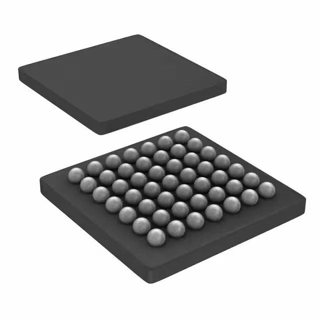
49-DSBGA — fine-pitch BGA, not for hand-soldering
The 49-DSBGA (2.8x2.8 mm) package is a 0.4 mm pitch BGA. That footprint demands a controlled reflow profile, solder-paste stencil, and X-ray inspection — this is not a hand-solder part.
The 16 MHz PLL and internal oscillator need to hold frequency across that span; the datasheet's timing numbers at the temperature extremes are what matter for the firmware's timing budget, not the 25°C typicals.
Listed as Active, so this is a current-production part. For new designs, the MSP430F2xx family has broad second-source and cross-compatibility across density options in the same DSBGA footprint, though no official pin-compatible alternate is listed in this entry.