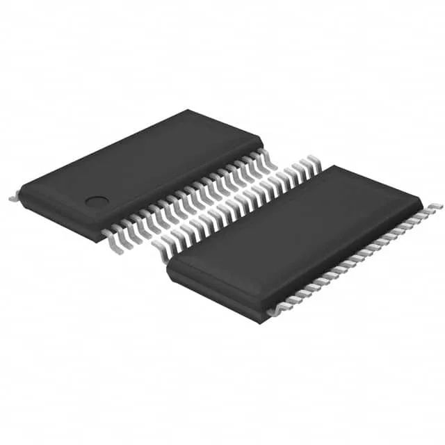
16-bit MCU for industrial and mixed-signal control
16 MHz core — timing budget and bus margin
The 16 MHz clock rate defines the instruction-cycle budget for the MSP430 CPU16. At 16 MHz, a single-cycle instruction executes in 62.5 ns, which gives comfortable margin for interrupt latency and real-time control loops.
Memory sizing — firmware and OTA fit
With 8 KB of Flash and 512 bytes of RAM, this part sits in the low-to-mid memory tier of the MSP430F2xx series. The 8 KB Flash can hold a modest bootloader plus application code for a sensor interface or a LIN slave node. The 512 B RAM limits buffering — a full 256-byte UART frame plus a 10-channel ADC scan will consume most of it, so the firmware engineer needs to budget stack and heap carefully. No wear-leveling is needed for the Flash endurance on a typical 10-year product life, but the erase granularity (usually 512-byte sectors in this family) matters for OTA update staging.