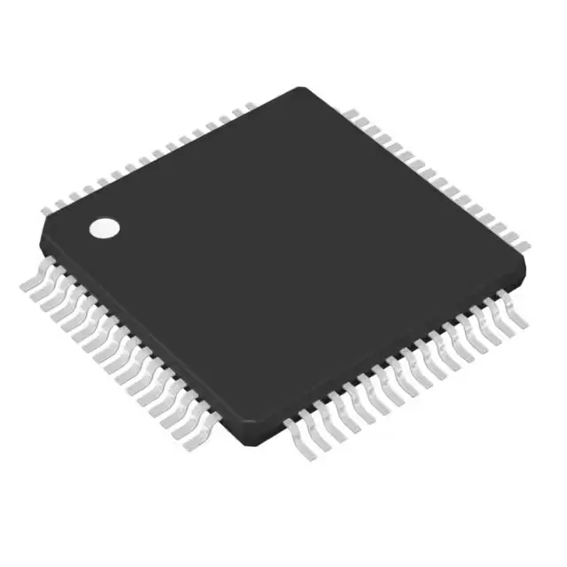
Bare-die MSP430 — what this package means for the build
The die form factor is the key differentiator here: no lead frame, no plastic overmold — the silicon is the component.
Die handling and assembly — the procurement angle
Because this part ships as a bare die, the usual SMT pick-and-place and reflow assumptions do not apply. The die requires a wafer-level or chip-on-board assembly process — wire bonding or flip-chip attach, plus die-attach epoxy or solder preform. That means the buyer needs to verify that their assembly house supports die-level handling, including wafer dicing, die pick, and bond-pad alignment. The supplier device package field lists 'Diesale', which indicates the die is sold as a known-good die, not as a sawn wafer. Plan for ESD-sensitive handling throughout the supply chain; the die has no protective overmold. The mounting type is surface mount, but that refers to the die being attached to a substrate, not to a conventional PCB pad layout.
Lifecycle status — still in active production
That said, the die form factor limits the pool of distributors who carry it — it is not a jellybean part stocked in high volume. No LTB risk to budget for the foreseeable future.
Memory and I/O — sizing the firmware and bus
The 8 KB Flash (8K x 8 plus 256 B) and 512 x 8 RAM set a clear boundary for firmware size and runtime data. The 512-byte RAM handles small buffers and a modest call stack; interrupt-heavy designs will need to watch stack depth. The 24 I/O pins give enough headroom for a keypad, a small LCD segment driver, or a sensor array, but not for a memory-mapped display or a parallel bus.