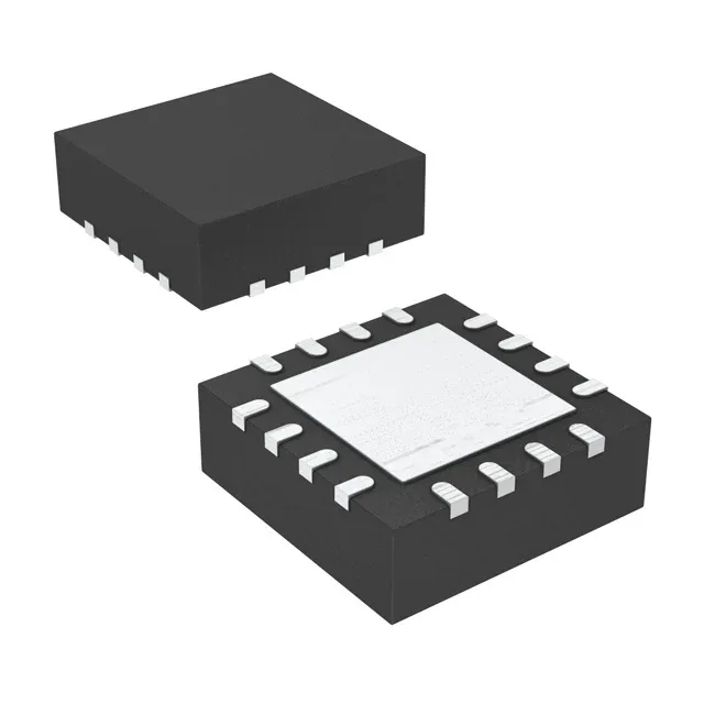
16 MHz core and 2 KB Flash — what the memory map means for firmware
The MSP430F2013IRSAT: The MSP430 CPU16 core runs at 16 MHz with a 16-bit data path. Program memory is 2 KB (2 K × 8 plus 256 bytes) of Flash, with 128 × 8 bytes of RAM. The 256-byte information memory segment is separate from the main Flash array and can hold calibration constants or boot parameters that survive a full-chip erase. For a firmware engineer: the 2 KB Flash limits the application to small control loops, sensor processing, or communication bridge tasks — the MSP430F2xx instruction set is dense, but a USB stack or RTOS kernel will not fit. The 128-byte RAM means stack depth and variable storage must be budgeted tightly; interrupt service routines with large local arrays will overflow.
Supply rails and decoupling on the 16-QFN exposed pad
Decoupling should be a 100 nF ceramic within 2 mm of each Vcc pin, plus a 4.7 µF bulk capacitor near the package. The exposed pad carries the return current for the I/O ring — a via array under the pad reduces ground inductance and improves EMC margin.
I/O, ADC, and serial interfaces
Ten general-purpose I/O pins are available, some shared with the peripheral functions. The 10-channel 16-bit ADC samples at up to 200 ksps in the MSP430F2xx — the 16-bit resolution is sigma-delta, not SAR, so the conversion time is longer than a 12-bit SAR ADC but the noise floor is lower for low-frequency sensor signals. Connectivity includes I²C and SPI, both implemented in hardware with dedicated shift registers. Brown-out detect (BOR), power-on reset (POR), PWM timer, and watchdog timer (WDT) are integrated — no external supervisor IC needed for basic reset and watchdog coverage.
This covers most factory-floor, outdoor enclosure, and under-cabinet applications, but not extended automotive (AEC-Q100 Grade 1 requires 125°C) or military (-55°C).