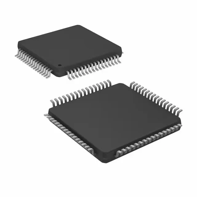
8 MHz core — clock tree and timing budget
The MSP430F148IPAG runs the MSP430 CPU16 core at 8 MHz, a 16-bit RISC architecture with a single-cycle multiplier. That 8 MHz clock is the internal DCO-driven speed; no external crystal is required, though one can be attached for a precise reference. At 8 MHz the instruction throughput is about 8 MIPS, enough for real-time control loops like sensor polling, PID updates, or protocol framing on SPI or UART. The flash wait state is zero at this clock — no pipeline stall penalty on code fetches.
Program memory is 48 KB of Flash (48K x 8 plus 256 B of info memory). That is a mid-range capacity in the MSP430x1xx family — enough for a moderate protocol stack plus application code, but tight if you are porting a full Bluetooth or CANopen stack. The RAM is 2K x 8 (2 KB), which constrains the stack depth and data buffer size. For designs that need more working memory, stepping up to the MSP430F149 (2 KB RAM, 60 KB Flash) is the natural move — same 64-TQFP footprint, same peripheral set.
Peripherals and I/O — what is on-chip
On-chip peripherals include POR, PWM, and WDT, plus an 8-channel 12-bit ADC and two serial interfaces (SPI and UART/USART). The ADC is a 12-bit SAR with eight external channels — enough for multi-sensor acquisition without an external mux. The serial interfaces share pins with GPIO, so plan the pin allocation against the 48-pin count before layout.