16-bit MSP430 for low-power control — 8 MHz, 4 KB Flash, 256 B RAM
On-chip peripherals include POR, PWM, and WDT, plus SPI and UART/USART connectivity for interfacing with sensors, displays, or a host controller. The slope A/D converter handles slow analog inputs without an external ADC.
Memory budget — what 4 KB Flash and 256 B RAM mean for your firmware
With 4 KB of Flash and 256 bytes of RAM, this MCU is not a candidate for complex protocol stacks or large lookup tables. The firmware fits a single control loop, a few state machines, and a modest communication buffer. The 256 x 8 RAM allocation means careful variable sizing — use byte-wide flags and avoid large arrays. The 256 B boot ROM area (included in the 4 KB + 256 B program memory) is typically reserved for the interrupt vector table and startup code. For designs that need more headroom, the MSP430x1xx family offers higher-density Flash options, but the pin-compatible migration path requires checking the exact package variant.
At the low end, 1.8 V operation keeps the MCU alive during battery discharge, extending system runtime. The MSP430 architecture is known for sub-µA sleep currents, though the exact standby draw depends on the clock configuration and enabled peripherals.
The ROHS3 compliance covers current environmental regulations across major markets.
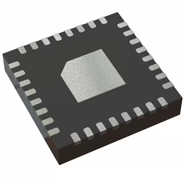
Package and footprint — 32-VQFN (5x5 mm)
Housed in a 32-VFQFN exposed-pad package (supplier device package 32-VQFN, 5x5 mm), this MCU takes minimal board area.