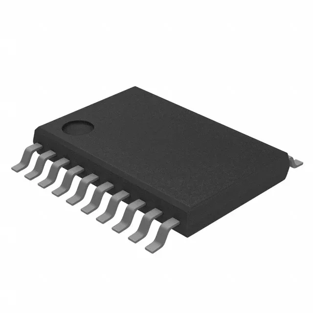
4 KB Flash and 256 B RAM — sizing the firmware and data budget
The 4 KB Flash (organized as 4K x 8 plus 256 bytes of information memory) is the program store for this MCU. For a BOM decision, this means the firmware image must fit within roughly 4 KB, including interrupt vectors and any bootloader stub. The 256 x 8 RAM is the working memory — stack, global variables, and small buffers. Designs that need more than a few hundred bytes of data space or a large lookup table will exceed this part's capacity; the MSP430F1121AIPW suits applications with lean control loops, state machines, or simple sensor readout tasks where code size is the tighter constraint.
8 MHz core speed — what it means for timing
The 8 MHz clock rate is the maximum CPU speed for this device. At 8 MHz, each instruction cycle (most single-cycle) takes 125 ns. This is adequate for polling sensors at kHz rates, handling UART communication at standard baud rates up to 115200, and running timer-based PWM or capture functions. It is not suited for high-speed DSP, video, or real-time control loops requiring sub-microsecond response — the 8 MHz ceiling sets the upper bound on throughput and interrupt latency.
Designs requiring extended temperature beyond 85°C or automotive qualification (AEC-Q100) should look at other MSP430 derivatives with higher temperature ratings.