Dual 24-bit ADC — the reason this MCU exists
That dual-ADC front end is the defining feature: it targets polyphase energy metering, precision weigh scales, and industrial sensor bridges where simultaneous sampling of two channels matters more than raw MIPS. The 12 MHz core clock is enough to run the ADC conversion engine and a lightweight metrology stack, but the 8 KB Flash and 512 B RAM leave no room for a general-purpose RTOS or complex protocol handling. Connectivity is limited to SPI and UART/USART — no I²C, no CAN, no USB. This is a purpose-built measurement controller, not a general-purpose MCU.
8 KB Flash, 512 B RAM — sizing the firmware budget
Program memory is 8 KB of Flash, with 512 bytes of RAM. For a metering application that means the calibration constants, the digital filter coefficients, and the communication protocol handler must all fit in that 8 KB. There is no external memory bus, so firmware size is a hard constraint. The 512 B RAM handles the ADC conversion results and a small transmit/receive buffer for SPI or UART. If the application needs data logging or over-the-air firmware updates, this part will not hold them — step up to the MSP430F5xx series with larger Flash options.
Package and I/O
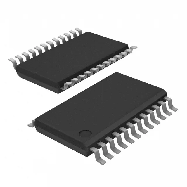
Housed in a 24-TSSOP package with a 4.40 mm body width, surface-mount only. The 11 I/O lines include the SPI and UART pins, plus a few GPIO for control signals and interrupts. The Brown-out Detect/Reset and watchdog timer are integrated, reducing external supervisor IC count. The PWM output can drive a simple buzzer or LED indicator, but there is no dedicated motor-control timer.
For dual-sourcing resilience, note that the MSP430AFE232IPW has no direct pin-compatible second source — the MSP430 family is TI-proprietary. If a second source is required for a high-volume production line, a functional equivalent would need a different architecture (e.g., an ARM Cortex-M0+ with a dual 24-bit ADC), which would require a board respin.