Texas Instruments LP5952TL-1.2/NOPB — Power Management (PMIC / Gate Driver)

LP5952TL-1.2/NOPB LDO Regulator, 1.2V Fixed, 350mA, 5-DSBGA

MPNLP5952TL-1.2/NOPB
End of Life

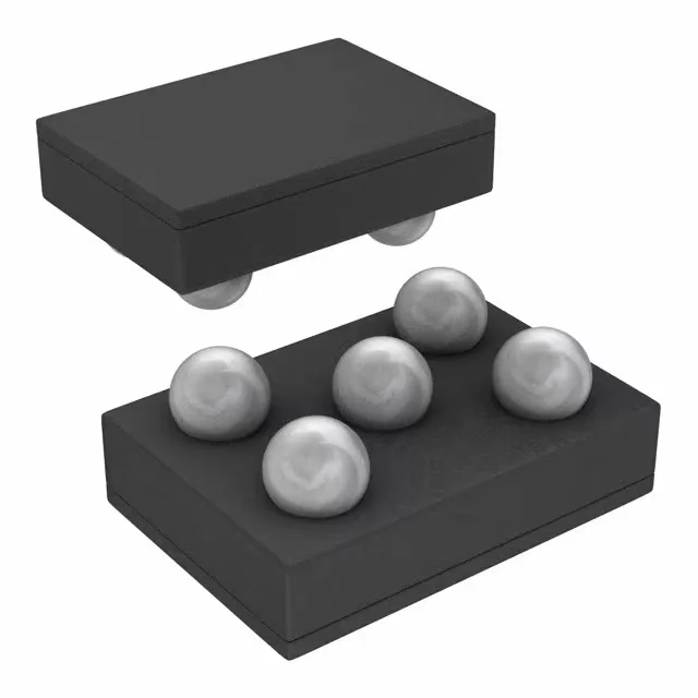
Texas Instruments LP5952TL-1.2/NOPB LDO regulator, fixed 1.2V output, 350mA, 5-WFBGA/DSBGA package, surface mount, active, ROHS3 compliant.

$0.92Ref. price · indicative, final on quote
Packaging5-WFBGA, DSBGA
RoHSROHS3 Compliant
Sourced new & surplus through independent channelsAuthenticity-screened · ESD-safe packingListing updated Aug 2026

Specifications

LP5952TL-1.2/NOPB specifications
ParameterValue
Output typeFixed
MountingSurface Mount
Voltage - input4.5V
Voltage dropout0.2V @ 350mA
Voltage - output (Min (Fixed))1.2V
Output current350mA
Current - supply100 µA
Current - quiescent28 µA
Operating temperature-40°C ~ 85°C
PSRR80dB ~ 64dB (10Hz ~ 100kHz)
PackageTape & Reel (TR); Cut Tape (CT)
Case5-WFBGA, DSBGA
Control featuresEnable
Protection featuresOver Current, Over Temperature, Short Circuit, Under Voltage Lockout (UVLO)
Number of regulators1
Output configurationPositive

Product details

350 mA LDO with 80 dB PSRR floor

The LP5952TL-1.2/NOPB is a single-output, positive fixed LDO from Texas Instruments delivering 350 mA at a 1.2 V output. Its PSRR holds 80 dB at 10 Hz and rolls off to 64 dB at 100 kHz, which means upstream switching noise from a buck converter or charge pump gets attenuated by a factor of several thousand before reaching the load rail — useful for powering sensitive analog front-ends or RF oscillators where supply ripple directly modulates the signal. Maximum dropout is 200 mV at the full 350 mA load, so a 1.4 V input rail provides the needed headroom with margin across temperature. Quiescent current sits at 28 µA typical, with a maximum supply current of 100 µA — low enough that the regulator's own draw does not dominate the battery budget in always-on sensor nodes.

5-DSBGA package and board-fit realities

Housed in a 5-bump DSBGA (5-WFBGA) measuring 1.41 x 1.08 mm, this is a wafer-level chip-scale package with no leads — the solder bumps are the entire interface. The 0.4 mm pitch and 0.5 mm nominal ball height mean the PCB land pattern must match the TI recommended footprint exactly; a 0.3 mm solder-mask-defined pad with a 0.25 mm solder-paste aperture is the usual starting point. The enable pin (active high) lets the system shut down the regulator when the load is idle — pulling it low drops the total draw to near zero, which matters for battery-powered products that spend most of their time in sleep. Protection includes over-current, over-temperature, short-circuit, and under-voltage lockout, so a downstream fault or a hot day does not cascade into a board failure.

Frequently asked questions

What is LP5952TL-1.2/NOPB's PSRR performance?

PSRR is specified at 80 dB at 10 Hz, rolling off to 64 dB at 100 kHz. This means the regulator attenuates low-frequency ripple by a factor of 10,000 and still provides 1,600× rejection at 100 kHz — enough to clean up most switching supply noise for analog loads.

What package does LP5952TL-1.2/NOPB use?

The part comes in a 5-bump DSBGA (5-WFBGA) package, supplier device package 5-DSBGA measuring 1.41 x 1.08 mm. It is a wafer-level chip-scale package with solder bumps — no leads, no exposed pad.