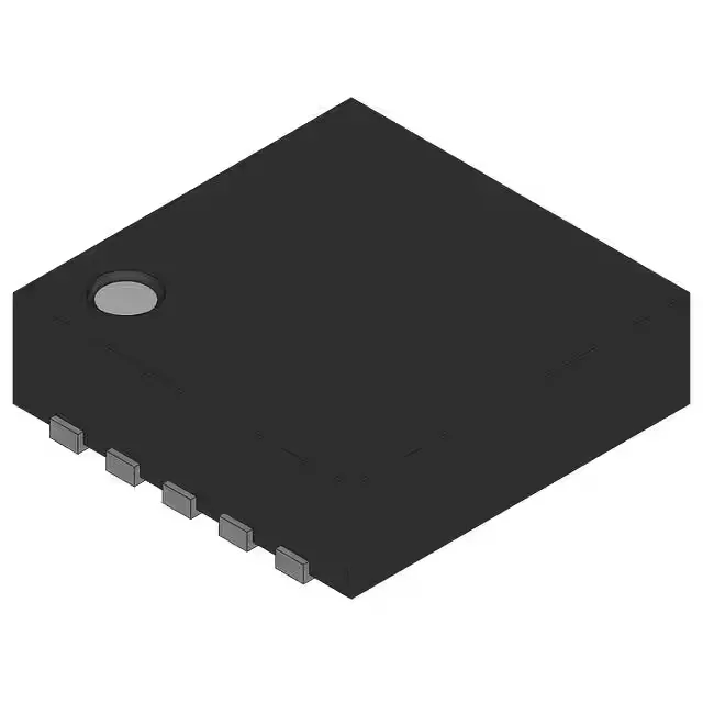
Package and board integration — 10-WSON (3x3 mm) exposed-pad LDO
The LP3996SD-2533 is supplied in a 10-WFDFN exposed-pad package, designated as 10-WSON (3x3 mm) per the supplier device package. The 0.5 mm pitch of the WSON package demands careful solder-paste stencil design to avoid bridging between adjacent pins. A 4-mil stencil with 1:1 aperture-to-land ratio is typical for this footprint class.
Dual-rail LDO with independent output currents and fixed voltages
The two rails share a common input (max 6 V) but regulate independently, so a single LP3996SD-2533 can power a 2.5 V analog front-end and a 3.3 V digital core from one upstream rail. The quiescent current is 100 µA typical, with a maximum supply current of 170 µA — low enough for battery-powered equipment where the LDO's own draw must not dominate the sleep-state budget.
PSRR across frequency — what the 58 dB to 45 dB range means for noise-sensitive loads
Power-supply rejection ratio is specified as 58 dB to 45 dB from 1 kHz to 20 kHz on one output, and 70 dB to 60 dB over the same frequency range on the other. The higher PSRR on the second output (70 dB at 1 kHz) makes it the preferred rail for analog circuitry such as ADC reference buffers or op-amp supplies, where 1 kHz switching noise from a preceding buck converter would otherwise couple into the signal path. At 20 kHz the PSRR drops to 45 dB on the lower-performance output — this means a 100 mVpp ripple at 20 kHz on the input appears as roughly 560 µVpp at the output. For a 16-bit ADC with a 3.3 V reference, that ripple contributes about 0.5 LSB of noise, which may be acceptable for industrial sensing but marginal for precision measurement.
Active lifecycle — no obsolescence risk for production builds
The over-temperature and short-circuit protection features provide fault tolerance for designs where the load may draw excess current during startup or fault conditions.