150 mA LDO with 100 mV dropout — the headroom budget
The LP3985ITLX-3.0/NOPB is a single-output, fixed 3 V linear regulator from Texas Instruments, rated for 150 mA continuous output. The 100 mV maximum dropout at full load sets the minimum input-to-output differential — if the input rail dips below 3.1 V at 150 mA, the output falls out of regulation.
PSRR profile — where it filters and where it doesn't
PSRR is specified at 50 dB at 1 kHz, dropping to 40 dB at 10 kHz. This means the regulator attenuates 1 kHz ripple on the input by a factor of ~316, but at 10 kHz the attenuation drops to ~100. Upstream switching noise above 10 kHz — from a buck converter running at 500 kHz or 1 MHz — passes through with significantly less rejection. If the load is an analog front-end sensitive to high-frequency ripple, a post-filter LC stage or a second LDO in cascade is worth budgeting into the BOM.
-40 to 125 °C — industrial and automotive temperature grade
The quiescent current is 150 µA typical, rising to 250 µA max — low enough for always-on battery-backed rails in an ECU or a sensor node that stays powered during ignition-off periods.
5-DSBGA — footprint and rework reality
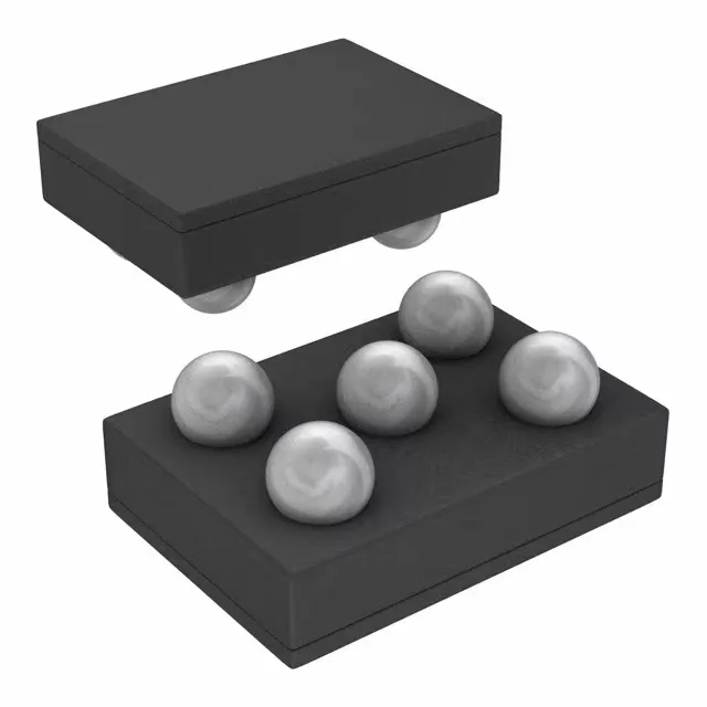
The package is a 5-bump wafer-level DSBGA measuring 1.41 mm × 1.08 mm. There is no mould compound body — the die backside is the top of the package. This means the solder joints are the sole mechanical attachment, and the board must be flat within the package footprint or the bumps crack during reflow. Rework requires a hot-air nozzle matched to the 1.4 mm × 1.1 mm outline; a standard 5 mm nozzle will heat adjacent passives and risk tombstoning. The 0.50 mm pitch demands a solder-mask-defined pad with a 0.25 mm opening and a 0.30 mm NSMD pad on the inner layers for consistent solder volume.
Protection set and control interface
Built-in protection covers over-current, over-temperature, and short-circuit events. The enable pin allows the output to be gated — pulling it low drops the quiescent current to near-zero, which is useful for sequencing multiple rails or for power-gating a load during sleep modes. The output is fixed at 3 V with no external resistor divider needed.
Active lifecycle — no end-of-life pressure
The part is RoHS3 compliant.