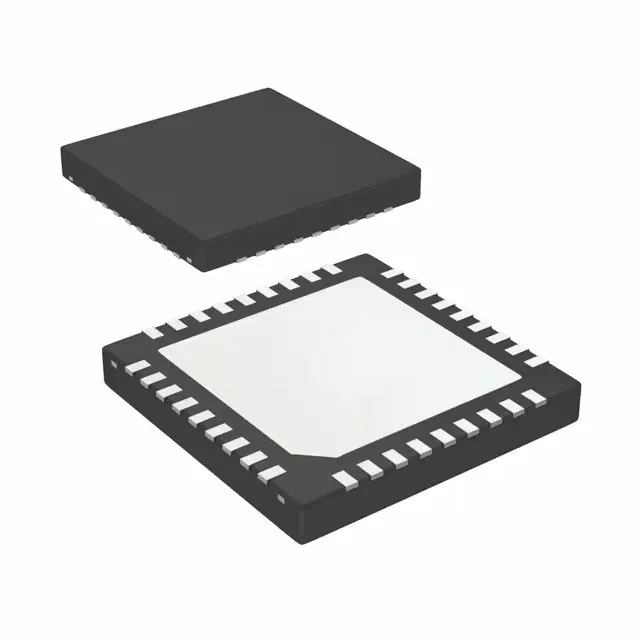
Texas Instruments LMX2571NJKT — Analog & Data Acquisition

LMX2571NJKT PLLatinum RF Frequency Synthesizer, 1.4 GHz

MPNLMX2571NJKT
End of Life

Texas Instruments PLLatinum™ LMX2571NJKT RF frequency synthesizer with integrated VCO, PLL with bypass, 1.4 GHz max frequency, 3.15V-3.45V supply, -40°C to 85°C, 36-WFQFN exposed pad.

$14.87Ref. price · indicative, final on quote
Packaging36-WFQFN Exposed Pad
StockContact for availability
MOQ1 pcs
  • 100% new & originalTraceable channels only — no refurbs, no pulls, no remarked parts.
  • Date & lot codes on quoteStated per line before you commit; label photos on request.
  • MSL-compliant ESD packingMoisture-sealed bags with indicator cards; reels photo-verified.
  • PayPal buyer protectionPay by T/T, PayPal or Payoneer — card payments covered end to end.

Specifications

LMX2571NJKT Technical Specifications
ParameterValue
TypeFrequency Synthesizer (RF)
SeriesPLLatinum™
Mounting typeSurface Mount
Voltage3.15V ~ 3.45V
Frequency1.4GHz
Operating temperature-40°C ~ 85°C
PLLYes with Bypass
InputClock, Crystal
OutputClock
PackageTape & Reel (TR); Cut Tape (CT)
Case36-WFQFN Exposed Pad
Divider (Multiplier)Yes/Yes
Number of circuits1
Ratio - Input:Output2:2
Differential - Input:OutputYes/No

Product details

RF synthesizer with VCO — what it does and where it fits

The Texas Instruments LMX2571NJKT is a PLLatinum™ RF frequency synthesizer with an integrated VCO, designed to generate clock signals up to 1.4 GHz from a crystal or clock input. It includes a PLL with bypass mode, which means the part can operate either as a closed-loop synthesizer or as a direct VCO — useful when you need to switch between locked precision and wideband modulation in the same design. The single-circuit device accepts two clock or crystal inputs and delivers two clock outputs, though the outputs are single-ended (no differential pair). Typical applications include wireless infrastructure, test equipment, and RF signal chains where a clean, programmable local oscillator is needed. The -40°C to 85°C temperature range covers most industrial and telecom enclosures, but not extended automotive or under-hood environments.

Supply rail tolerance — plan for a clean 3.3 V

The supply range is 3.15 V to 3.45 V.

Package and mounting — 36-WQFN with exposed pad

The LMX2571NJKT comes in a 36-lead WFQFN with an exposed pad (6x6 mm body). The exposed pad is the thermal and electrical ground path — it must be soldered to a PCB ground plane with adequate thermal vias. Reflow is the intended assembly method; hand-soldering this package on site is possible with a hot-air station and a fine-tip iron for the perimeter leads, but the pad underneath needs paste or a preform. No lab bench required, but a standard reflow profile is the reliable path. The part is surface-mount only; no through-hole variant exists.

Lifecycle and sourcing — active, no LTB pressure

The LMX2571NJKT carries an Active product status with ROHS3 compliance. If you are qualifying this into a new BOM, there is no imminent obsolescence risk to plan around.

Frequently asked questions

What is the output frequency range of LMX2571NJKT?

The maximum output frequency is 1.4 GHz. The part synthesizes clock signals from a crystal or clock input up to that ceiling.