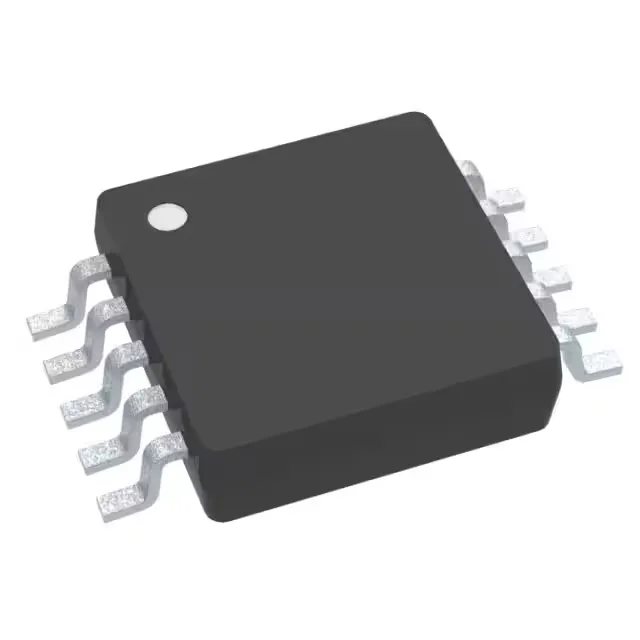
Texas Instruments LMV712Q1MM/NOPB — Logic ICs

TI LMV712Q1MM/NOPB Automotive Dual Op-Amp, 5 MHz, 5 V/µs

MPNLMV712Q1MM/NOPB
End of Life

Texas Instruments LMV712Q1MM/NOPB, Automotive AEC-Q100 series, dual general-purpose op-amp, 5 MHz gain bandwidth, 5 V/µs slew rate, rail-to-rail output, 2.7 V to 5.5 V supply, -40°C to 125°C, 10-VSSOP package.

$2.34Ref. price · indicative, final on quote
Packaging10-TFSOP, 10-MSOP (0.118", 3.00mm Width)
StockContact for availability
MOQ1 pcs
  • 100% new & originalTraceable channels only — no refurbs, no pulls, no remarked parts.
  • Date & lot codes on quoteStated per line before you commit; label photos on request.
  • MSL-compliant ESD packingMoisture-sealed bags with indicator cards; reels photo-verified.
  • PayPal buyer protectionPay by T/T, PayPal or Payoneer — card payments covered end to end.

Specifications

LMV712Q1MM/NOPB Technical Specifications
ParameterValue
SeriesAutomotive, AEC-Q100, LMV®
Output typeRail-to-Rail
Mounting typeSurface Mount
Amplifier typeGeneral Purpose
Voltage - input offset400 µV
Voltage - supply span5.5 V
Current - supply1.22mA (x2 Channels)
Current - input bias5.5 pA
Current - output (Channel)50 mA
Operating temperature-40°C ~ 125°C
Gain bandwidth product5 MHz
PackageTape & Reel (TR); Cut Tape (CT)
Slew rate5V/µs
Case10-TFSOP, 10-MSOP (0.118\", 3.00mm Width)
Number of circuits2

Product details

At 5 MHz gain-bandwidth, this amplifier closes a gain-of-10 stage with a 500 kHz closed-loop bandwidth — enough for anti-aliasing filters ahead of a 12-bit ADC sampling at 200 kSPS. The 5 V/µs slew rate means a 2 V step settles in about 400 ns, so the output doesn't limit the ADC's acquisition time. For slower signals like temperature or pressure sensor outputs, the bandwidth margin lets you add a second-order low-pass filter without eating into the passband. Input bias current is 5.5 pA typical, which keeps DC errors low when the source impedance is in the tens of kilohms — a common case with piezoresistive pressure sensors or thermistors. The 400 µV maximum input offset voltage is typical for a general-purpose automotive op-amp; if your application needs sub-100 µV offset, you'd step to a zero-drift type, but for most sensor interface circuits this is within the system calibration budget.

Package and footprint for the board designer

The surface-mount package is compatible with standard reflow profiles. Each channel can source or sink 50 mA, enough to drive the input of a downstream ADC or a modest analog multiplexer directly. The supply current is 1.22 mA per channel typical, so the dual amplifier draws about 2.44 mA total. In an always-on automotive module that must survive key-off draws, that's manageable — the part won't dominate the sleep budget if the rest of the circuit is properly gated.

Lifecycle and compliance

The "NOPB" suffix confirms lead-free (No Pb) construction, which matches current RoHS requirements. The AEC-Q100 qualification is documented on the series level, so the part is production-released for automotive supply chains.

Frequently asked questions

Is LMV712Q1MM/NOPB AEC-Q100 qualified?

Yes, the LMV712Q1MM/NOPB is part of the Automotive, AEC-Q100 series from Texas Instruments. The Q1 suffix in the order code designates the automotive-grade variant, qualified for use in production automotive electronics.

Does LMV712Q1MM/NOPB have a replacement?

The LMV712Q1MM/NOPB is currently an active product with no official end-of-life notice or successor part announced. For a higher-speed alternative in the same package, the TLV9362IDDFR offers 10.6 MHz GBW and 25 V/µs slew rate, also AEC-Q100 qualified, but it draws about 2.6 mA per channel — roughly double the quiescent current.

Is LMV712Q1MM/NOPB RoHS compliant?

Yes, the part is ROHS3 compliant. The NOPB suffix indicates lead-free (No Pb) construction, and the ROHS3 compliance covers the full substance restriction set.