Parametric anchor for the BOM line
The LMV652MMX/NOPB: Each channel draws 118 µA quiescent current, so the total supply draw for both amplifiers is 236 µA. For a battery-powered sensor node running off a coin cell, that quiescent load sits well below the self-discharge rate of a CR2032 — the op-amp is not the dominant drain in the sleep budget.
Supply rails and output swing
For driving heavier loads, buffer the output with a transistor stage.
Temperature grade and package options
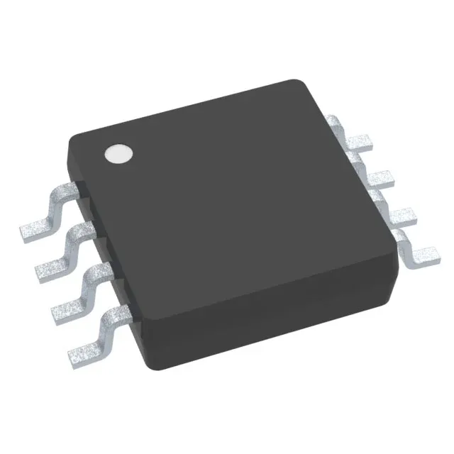
The 8-VSSOP package (3.00 mm width) is a space-saving footprint for dense PCBs, and the device is also available in 8-TSSOP and 8-MSOP variants.
DC precision and input characteristics
Input offset voltage is 100 µV typical — adequate for 8- to 10-bit signal chains without auto-zero calibration. Input bias current is 80 nA, which matters if the source impedance exceeds 100 kΩ; for a 10 kΩ sensor, the voltage error from bias current is under 1 mV.