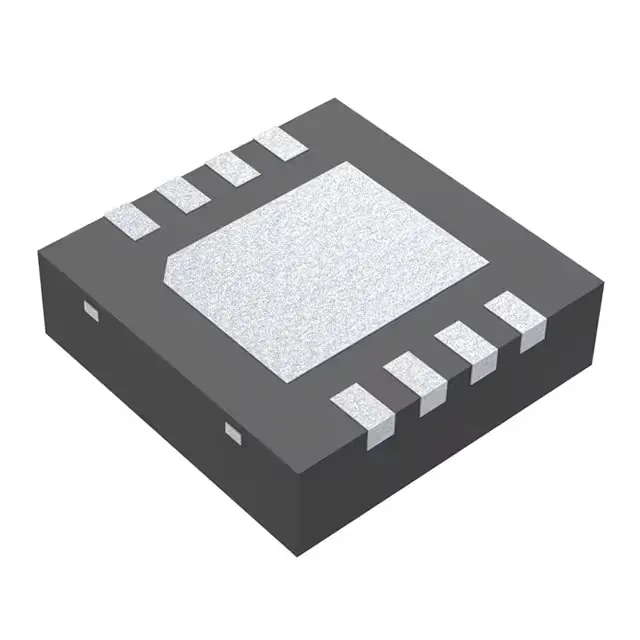
The LMV112SD/NOPB is an active-production clock buffer/driver from Texas Instruments, listed with current lifecycle status. This means the part is still in the manufacturer's active portfolio and can be sourced through authorized distribution channels. For BOM planning, there is no last-time-buy window or obsolescence risk on the immediate horizon.
1:1 fanout, 40 MHz ceiling, dual-circuit
This is a 1:1 clock buffer with a maximum frequency of 40 MHz. The 40 MHz ceiling sets the upper limit for the clock distribution tree; downstream logic must stay within this rate for clean edge propagation. Two independent buffer circuits are integrated in a single 8-WSON (3x3) package. Each circuit provides its own clock input and output, allowing the part to buffer two separate clock signals or split a single input across two isolated paths. This wide range makes the buffer suitable for mixed-voltage systems where the clock source and the load operate at different supply levels, as long as both stay within the same VDD rail.
Industrial temperature grade, non-differential signalling
This qualifies it for factory-floor equipment, outdoor telecom enclosures, and automotive cabin applications that see temperature swings outside the commercial 0°C to 70°C range. Both the input and output are single-ended (non-differential), as indicated by the No/No entry for differential input and output. This means the buffer accepts and delivers standard CMOS/TTL-level clock signals, not LVDS or CML. The single-ended interface simplifies PCB routing but is more susceptible to common-mode noise on long traces compared to differential signalling. The device is supplied in an 8-WFDFN exposed-pad package (also designated 8-WSON 3x3 mm). The exposed pad on the underside provides a low thermal resistance path to the PCB ground plane — essential for heat dissipation when the buffer is driving high-capacitance loads at the maximum frequency. The datasheet's recommended land pattern should include a thermal via array under the pad.
Sourcing and compliance documentation
Texas Instruments provides standard compliance documentation for the LMV112SD/NOPB, including the ROHS3 compliance declaration. As an active-production part, the LMV112SD/NOPB is available through authorized TI distribution channels. No stock-holding claim is made here — availability is verified per RFQ.