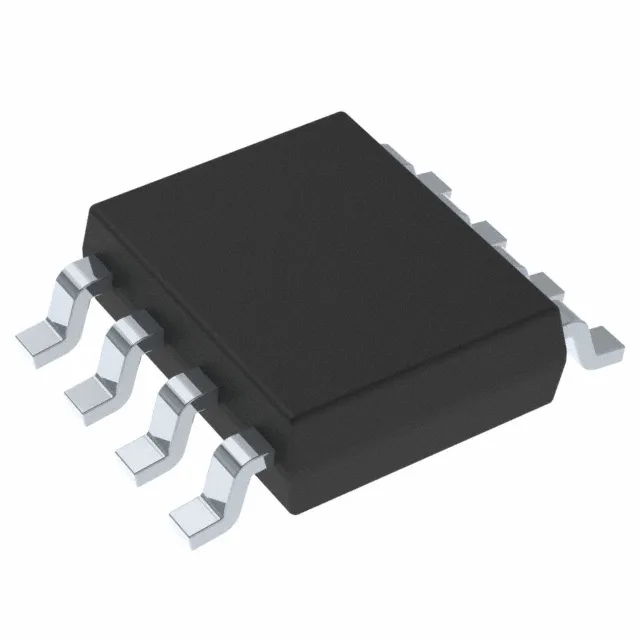
60 V input, 2 A output — the wide-VIN workhorse
The LMR16020PDDA is a SIMPLE SWITCHER® non-synchronous step-down regulator that takes 4.3 V to 60 V on the input and delivers an adjustable output from 0.8 V up to 50 V at 2 A continuous. The 60 V abs-max input means it handles 24 V industrial rails with headroom for transients, and the 0.8 V feedback reference lets it power modern 1.2 V or 1.8 V logic cores directly. Because it is non-synchronous (no internal low-side FET), the BOM needs an external Schottky catch diode. This adds a component but keeps the cost down and lets you select a diode with the reverse recovery characteristic that matches your switching frequency.
Switching frequency range — inductor sizing lever
The LMR16020PDDA switches between 200 kHz and 2.5 MHz, set by a single resistor to ground. Running at 2.5 MHz shrinks the inductor to a 4.7 µH or 10 µH footprint — good for space-constrained boards — but pushes switching losses higher. Dropping to 200 kHz improves efficiency by a few points at the cost of a larger 47 µH or 100 µH inductor. The frequency range overlaps with the AM broadcast band at the low end; if your system has sensitive RF front-ends, plan the layout so the switch node and inductor loop do not couple into the antenna path.
8-SO PowerPad — rework and thermal reality
That pad is the main heat path — the junction-to-board thermal resistance drops significantly when the pad is soldered to a copper pour on the PCB. A 1 oz copper plane of at least 2 in² under the pad keeps the junction below 125°C at 2 A output. From a rework standpoint, the PowerPad is forgiving: the leads are on 1.27 mm pitch, so a standard chisel tip and flux wick clear the pads cleanly. The pad itself needs a stencil aperture about 70% of the pad area to avoid voiding — too much paste and the part floats, too little and the thermal connection suffers. A hot-air station at 320°C with a small nozzle lifts the part without lifting the pad, provided the board was baked per J-STD-033.
Temperature grade and environment
The junction temperature, not the ambient, is the binding limit — derate output current above 85°C ambient per the thermal derating curve in the datasheet.