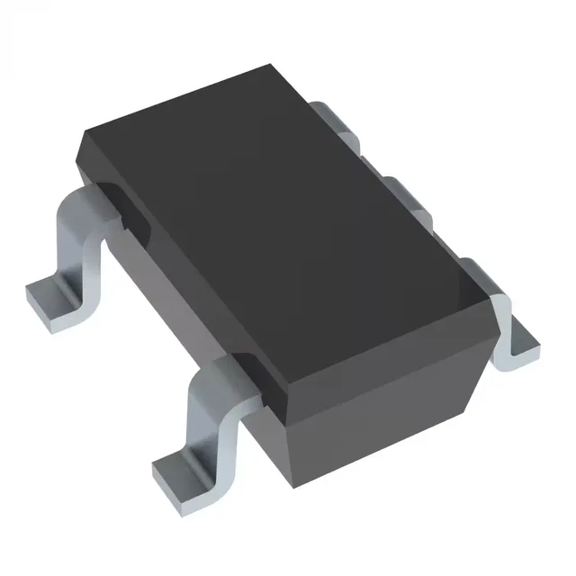
1.5 A buck, 1.6 MHz — the load and the loop
The LMR10515XMFE/NOPB: Switching at 1.6 MHz, the converter keeps the inductor and output capacitor small enough for the SOT-23-5 footprint, but the high frequency means the loop compensation and layout parasitics matter more than at lower switching speeds.
Output range and topology constraints
The adjustable output spans 0.6 V to 4.5 V, so the same part serves a 1.2 V core rail, a 1.8 V I/O rail, or a 3.3 V peripheral bus from a single BOM line. This is a non-synchronous buck — the low-side switch is an external Schottky diode, not an internal FET. The diode forward drop adds a few percent efficiency loss at light load, but the external diode lets the designer choose a part with the right Vf and thermal rating for the application.
Housed in a 5-lead SOT-23 (SC-74A, SOT-753), the package footprint is 2.9 mm × 1.6 mm — the limiting factor for board area is the input and output capacitors, not the IC itself. The exposed pad on the bottom side must be soldered to the PCB ground plane for thermal relief; without a thermal via array under the pad, the junction temperature rise above ambient at 1.5 A output can exceed the 125 °C limit in still air.