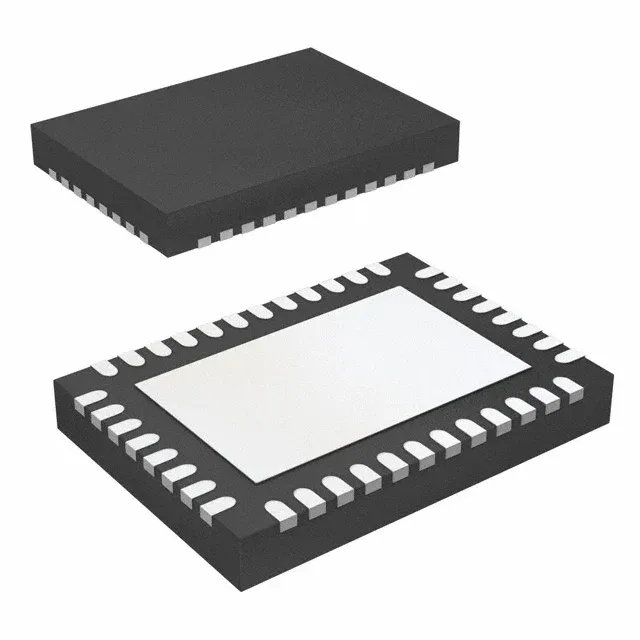
2:6 LVDS fanout buffer — 2 GHz differential path
The LMK1D2106RHAR is a 2:6 clock buffer from Texas Instruments, accepting differential or single-ended inputs (CML, HCSL, LVCMOS, LVDS, LVPECL) and delivering six LVDS output copies. The 2 GHz maximum frequency covers the fastest reference clocks for SerDes, FPGA transceivers, and RF sampling converters — the buffer's additive jitter at that edge is the figure that determines whether the downstream PLL stays locked. Two independent fanout banks each take one input and distribute to three LVDS outputs, giving a total 2:6 ratio. The differential input-to-output path is fully differential (Yes/Yes), so the part preserves signal integrity across the fanout tree without converting to a single-ended rail internally.
Supply voltage and temperature range
The core and output rails share the same supply pin — the buffer operates from a single rail within any of these bands, so the board only needs one regulated voltage for the device.
40-VQFN package and board integration
Surface-mount package supplied in Tape & Reel, compatible with standard pick-and-place and reflow processes. The 0.5 mm pitch QFN demands a solder-paste stencil aperture that matches the datasheet footprint recommendation — the pad geometry affects both solder-joint reliability and thermal resistance.