Active buffer for clock-tree fanout
The LMK1C1102DQFT is a 1:2 clock buffer from Texas Instruments, accepting a single LVCMOS input and delivering two LVCMOS outputs at up to 250 MHz. The 1:2 ratio means one input fans out to exactly two copies — useful for splitting a reference clock to two downstream PLLs or ASICs without loading the source. It operates across three supply voltage ranges — 1.71V to 1.89V, 2.375V to 2.625V, and 3.135V to 3.465V — covering 1.8V, 2.5V, and 3.3V nominal rails. No level-shifting is needed when the buffer runs on the same rail as the upstream clock source.
Package footprint and supply rails
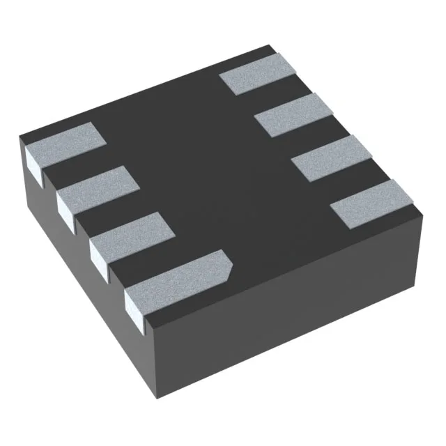
Housed in an 8-WFDFN package (2x2 mm WSON), the LMK1C1102DQFT occupies minimal board area. The exposed thermal pad on the 8-WSON (2x2) requires a solder-land pattern matching the supplier device package recommendation for proper heat dissipation and mechanical strength. The non-differential input and output (LVCMOS) mean this buffer is a straight-through fanout — no CML, LVPECL, or LVDS translation. The single-circuit design handles one clock path at a time.
This is a current catalog part, not a phase-out or NRND line. Availability is confirmed per RFQ. No through-hole or tray variants exist for this order code.