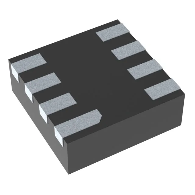
The Texas Instruments LMK1C1102DQFR is a 1:2 clock buffer — a single-input, dual-output fanout buffer that takes LVCMOS or standard clock signals and distributes them to two loads with minimal added jitter. It is not a PLL, not a jitter cleaner, and not a level translator; its job is to regenerate a clean copy of the incoming clock edge at up to 250 MHz. The part operates across three supply-voltage ranges — 1.71V to 1.89V, 2.375V to 2.625V, and 3.135V to 3.465V — covering the common 1.8V, 2.5V, and 3.3V nominal rails. This lets a single BOM line serve multiple voltage domains in a mixed-rail design.
The LMK1C1102DQFR comes in an 8-WSON package (2x2 mm body, 0.5 mm pitch) — a small, low-profile leadless package that saves board area but demands careful rework. Without those vias, the pad can stay cold and the part may not wet properly.