Two PLL domains for independent clock trees
The LMK05028RGCR integrates two independent PLL circuits (cites:,), each capable of locking to a different reference and generating separate output frequency domains. This matters when a line card needs one clean clock for the 10 GbE MAC and another for the backplane SerDes — the two PLLs let you run them from a common reference without sharing the same loop bandwidth or phase-noise profile. The 4:8 input-to-output ratio (cites:) means four reference inputs can be monitored for hitless switching while eight differential or single-ended outputs distribute the cleaned clocks. A typical deployment would feed two references from redundant GPS-disciplined oscillators and map the eight outputs across multiple ASICs, FPGAs, and PHYs.
Signal standard flexibility across the clock tree
Both the input and output banks accept CML, HCSL, LVDS, and LVPECL levels, with LVCMOS available on the output side (cites:,). This eliminates the need for external level translators when interfacing a 100 MHz LVDS oscillator to a downstream CML SerDes — the LMK05028RGCR handles the translation inside the package. The dual frequency maxima — 200 MHz on one path and 750 MHz on the other (cites:) — reflect the two PLL output dividers. The 750 MHz path is typically used for high-speed SerDes reference clocks where the phase noise at the carrier offset matters more than the absolute frequency.
Supply rail planning for the three voltage domains
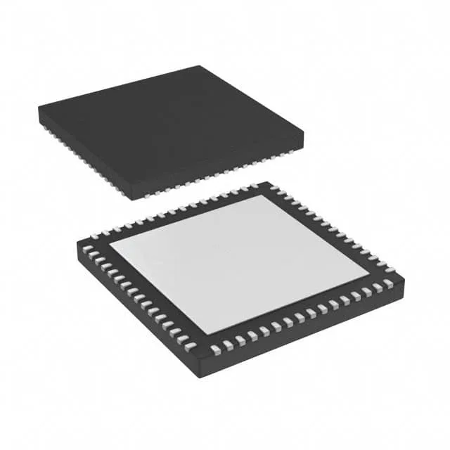
The 64-VFQFN package with exposed pad (cites:,) provides a thermal path through the ground paddle. The datasheet's recommended land pattern includes a 9×9 mm pad with via array — the via count and copper plane area under the pad determine the thermal resistance for the 2.5 W typical dissipation at 85°C ambient.
The part is sourced to order against BOM quantities.