PLL core and frequency ceiling
The LMK04906BISQE/NOPB integrates a PLL frequency synthesizer (PLL: Yes) capable of generating clocks up to 2.6 GHz — this is the headline spec that determines whether the part can serve as the reference for a 10 GbE SerDes, a JESD204B ADC/DAC sampling clock, or a high-speed FPGA transceiver. The 2.6 GHz ceiling covers most RF and baseband clocking needs in wireless infrastructure and instrumentation. The 3:6 input-to-output ratio means three independent clock inputs (LVCMOS, LVDS, or LVPECL) can be routed to any of six outputs, with differential signaling supported on both sides (Differential - Input:Output: Yes/Yes). This allows redundant clock sources or multiple frequency domains from a single device — useful in redundant timing trees for telecom or data center equipment.
I/O flexibility and supply rails
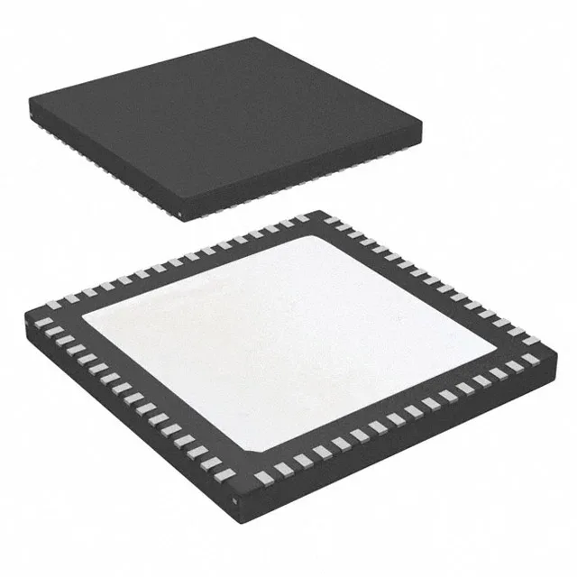
Input and output standards span LVCMOS, LVDS, and LVPECL — the three most common clock signaling families in digital and RF systems. This means the same part can interface with a crystal oscillator (LVCMOS), a differential PECL source, or an LVDS clock fanout without external level translation, simplifying the BOM and PCB layout. The supply voltage range is 3.15 V to 3.45 V — a tight 300 mV window that requires a clean 3.3 V rail with less than 5% ripple. The 64-WFQFN exposed pad package (9x9 mm) demands a solid thermal and ground connection through the center pad; the datasheet's recommended land pattern should be followed exactly to keep the PLL phase noise within spec.
Industrial temperature and active lifecycle
The industrial grade also covers most commercial networking hardware with margin. Texas Instruments lists this part as Active. Sourced to order through authorized and independent distribution; availability and current pricing confirmed at RFQ.