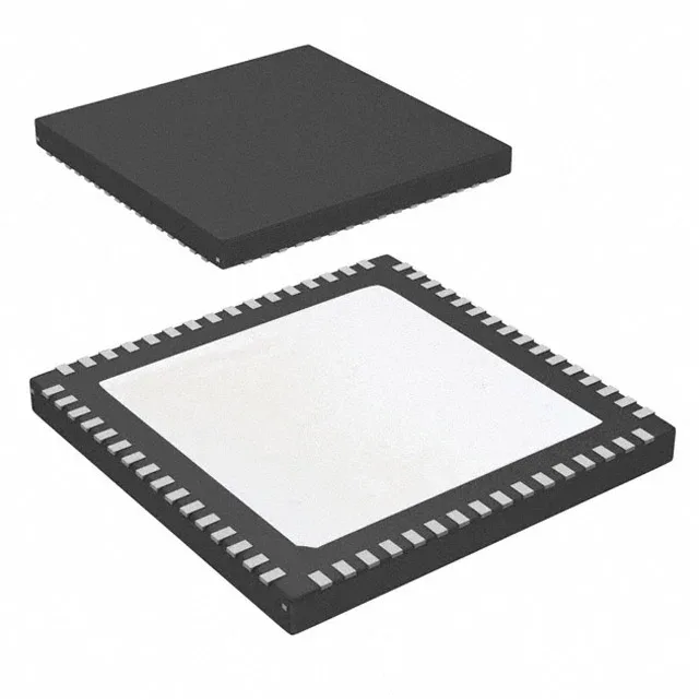
Texas Instruments LMK04828BISQ/NOPB — Clock & Timing ICs

LMK04828BISQ/NOPB PLLatinum Jitter Cleaner, 3.08 GHz

MPNLMK04828BISQ/NOPB
Active

Texas Instruments PLLatinum™ jitter cleaner PLL, LMK04828BISQ/NOPB, 3.08 GHz max frequency, 3:15 input:output ratio, LVCMOS/LVDS/LVPECL inputs, HSDS/LCPECL/LVCMOS/LVDS/LVPECL outputs, 64-WQFN (9x9) package, -40 to 85°C operation.

$26.6200Ref. price · indicative, final on quote
Packaging64-WFQFN Exposed Pad
RoHSROHS3 Compliant
SeriesPLLatinum™
Independent supplier — new & surplus stockAuthenticity-screened · ESD-safe packingListing updated Aug 2026

Specifications

LMK04828BISQ/NOPB specifications
ParameterValue
TypeJitter Cleaner
SeriesPLLatinum™
MountingSurface Mount
Supply voltage3.15V ~ 3.45V
Frequency - max3.08GHz
Operating temperature-40°C~85°C
PLLYes
InputLVCMOS, LVDS, LVPECL
OutputHSDS, LCPECL, LVCMOS, LVDS, LVPECL
PackageTape & Reel (TR); Cut Tape (CT)
Case64-WFQFN Exposed Pad
Divider (Multiplier)Yes/No
Number of circuits1
Ratio - Input:Output3:15
Differential - Input:OutputYes/Yes

Product details

The Texas Instruments LMK04828BISQ/NOPB is a dual-PLL jitter cleaner in the PLLatinum™ family, built to scrub phase noise from reference clocks and distribute clean timing to ADCs, DACs, FPGAs, or RF converters. It takes in LVCMOS, LVDS, or LVPECL references and fans out up to fifteen outputs in HSDS, LCPECL, LVCMOS, LVDS, or LVPECL formats — enough to clock an entire mixed-signal board from one device. The 3.08 GHz maximum output frequency covers L-band and C-band local-oscillator distribution, while the 3:15 input-to-output ratio means you can select among three reference sources and route the cleaned clock to every high-speed converter on the board without external fanout buffers. It lives in a 64-pin WQFN (9x9 mm) with an exposed pad for thermal relief, and runs off a 3.15 V to 3.45 V supply rail — a tight tolerance that wants a low-noise LDO, not a switcher feeding it directly.

Lifecycle and sourcing — no LTB worry here

What the 3.08 GHz and the output formats mean for your clock tree

Having both differential (LVDS, LVPECL, HSDS, LCPECL) and single-ended (LVCMOS) outputs on the same chip simplifies a mixed-logic board: the FPGA gets LVDS, the ADC gets LVPECL, and a slow monitoring clock comes out as LVCMOS — all from one device. The 3:15 input:output ratio with differential I/O throughout means you can hit fifteen destinations with one cleaned clock, saving board area and reducing the number of PLLs you need to qualify.

Frequently asked questions

Is LMK04828BISQ/NOPB obsolete or end-of-life?

No — the lifecycle status is active (current production). There is no end-of-life notice or last-time-buy schedule on this part. It is ROHS3 compliant and fully in production.

Does LMK04828BISQ/NOPB support LVDS output?

Yes — LVDS is one of the five supported output formats, alongside HSDS, LCPECL, LVCMOS, and LVPECL. You can mix output types across the fifteen outputs.