PLLatinum jitter cleaner — what the PLL and 1.536 GHz ceiling mean for your clock tree
The LMK04808BISQ/NOPB is a PLL-based jitter cleaner from TI's PLLatinum series — the PLL locks to a reference and filters out phase noise, so what comes out is a cleaner clock than what went in. The 1.536 GHz max output frequency means it can generate clocks for high-speed ADCs, FPGAs, or SerDes transceivers that need a low-jitter reference at or below that ceiling. With two reference inputs and fourteen clock outputs (2:14 ratio), this part fans out a cleaned-up clock to multiple destinations on the board — no need for separate buffers downstream for most designs.
I/O flexibility and supply rail — what the 3.15–3.45 V and LVCMOS/LVDS/LVPECL mean for board integration
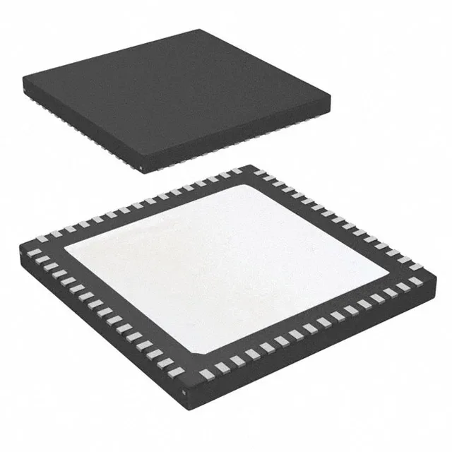
The supply range is tight — 3.15 V to 3.45 V — so this part expects a clean regulated 3.3 V rail, not a noisy system bus. The 64-WFQFN with exposed pad (9x9 mm) needs the thermal pad soldered to a PCB ground plane; that's both the thermal path and the electrical ground reference for the PLL's analog core. Inputs and outputs accept or drive LVCMOS, LVDS, or LVPECL levels — that covers the three most common clock signaling standards in base-station, test, and communications gear. The differential I/O capability (Yes/Yes) means the high-frequency outputs can run as LVDS or LVPECL pairs, keeping signal integrity intact over longer board traces.
Active lifecycle and industrial temperature range
The base product number is LMK04808, so variant-specific marking (BISQ/NOPB) indicates the tape-and-reel packaging and RoHS compliance (NOPB suffix).