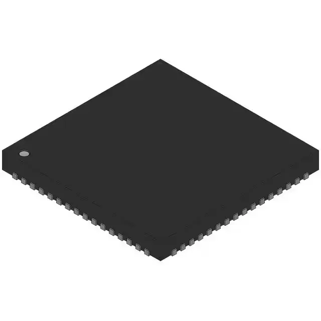
1.536 GHz jitter cleaner with 14 outputs
The LMK04806BISQX/NOPB is a PLLatinum jitter cleaner from Texas Instruments, designed to reduce phase noise on a reference clock and distribute clean timing to multiple downstream devices. Its 1.536 GHz max output frequency covers the clock rates required by JESD204B high-speed data converters and RF transceivers. With a 2:14 input-to-output ratio, the part accepts two reference inputs and delivers 14 clock outputs — enough to clock an entire multi-channel ADC or DAC board from a single device. The outputs are configurable as LVCMOS, LVDS, or LVPECL, so a mix of high-speed serial lanes and single-ended control clocks can share the same IC.
What the 1.536 GHz ceiling means for your clock tree
The 1.536 GHz maximum output frequency is the upper limit of the VCO and divider chain. For a 122.88 MHz reference (common in wireless infrastructure), the internal PLL multiplies up to the VCO frequency, then divides down to the target output rate. The integrated PLL (Yes) means the device synthesizes the output from the reference — it does not require an external VCXO for the jitter-cleaning loop.
The 64-WFQFN exposed-pad package (9x9 mm body) requires a thermal via array under the center pad to conduct heat to the ground plane. The exposed paddle is the primary thermal path — without adequate vias, the junction temperature rises above the 85°C ambient limit even at moderate output loading. Differential inputs and outputs (Yes/Yes) mean the high-frequency clock lanes use LVDS or LVPECL pairs, which need 100-ohm differential trace impedance on the PCB. The LVCMOS outputs, when used, should be terminated near the load to avoid reflections at the edge rates this part can produce.
Active lifecycle — sourcing posture
Sourced through independent distribution channels. The tape-and-reel packaging (TR) is the standard delivery format for the 64-WQFN package.