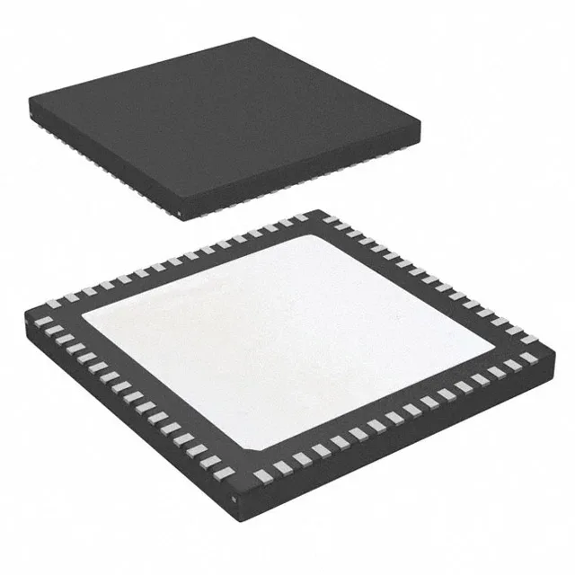
What the PLL and jitter-cleaner architecture means for a timing chain
The LMK04805BISQX/NOPB integrates a PLL (Yes) configured as a jitter cleaner — it locks to a reference clock and filters out phase noise above the loop bandwidth, delivering a cleaned clock to downstream converters, FPGAs, or SerDes transceivers. With a 2:14 input-to-output ratio, a single reference clock (LVCMOS, LVDS, or LVPECL) feeds the PLL, and fourteen outputs distribute the cleaned clock across multiple board domains — useful in a base station or ADC array where one clean master clock fans out to many lanes. The 1.536 GHz maximum frequency covers common telecom and data-converter clock rates, including 153.6 MHz reference multiples for LTE/5G NR and 1.2288 GHz for JESD204B subclass 1 deterministic latency.
Supply rails, temperature grade, and package fit
The 3.15 V to 3.45 V supply range is narrow — the PLL's VCO and charge pump are sensitive to supply ripple; a dedicated LDO feeding this rail is typical, with the exposed pad (64-WQFN, 9x9 mm) soldered to a quiet ground plane for thermal and substrate-noise management. Industrial temperature range (-40°C to 85°C) means the device holds lock and jitter performance across outdoor telecom cabinets and industrial enclosures without active cooling. Differential inputs and outputs (Yes/Yes) support LVDS and LVPECL signalling — the common-mode rejection rejects ground bounce and supply noise picked up across a backplane or long PCB trace.
Active lifecycle — no last-time-buy pressure
The base product number LMK04805 identifies the device family; the suffix BISQX/NOPB indicates the tape-and-reel packaging and RoHS-compliant build (NOPB = no lead).