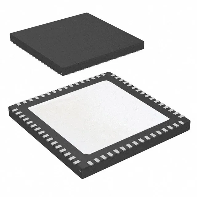
Texas Instruments LMK04803BISQ/NOPB — Clock & Timing ICs

LMK04803BISQ/NOPB PLL Jitter Cleaner – 1.536 GHz

MPNLMK04803BISQ/NOPB
Active

Texas Instruments PLLatinum™ series, IC JITTER CLEANER, PLL Yes, Type Jitter Cleaner, Input LVCMOS, LVDS, LVPECL, Output LVCMOS, LVDS, LVPECL, Frequency - Max 1.536GHz, Number of Circuits 1, Ratio - Input:Output 2:14, Voltage - Supply 3.15V ~ 3.45V, Operating Temperature -40°C ~ 85°C, Package / Case 64-WFQFN Exposed Pad, Supplier Device Package 64-WQFN (9x9), Mounting Type Surface Mount.

$19.7000Ref. price · indicative, final on quote
Packaging64-WFQFN Exposed Pad
RoHSROHS3 Compliant
SeriesPLLatinum™
Independent supplier — new & surplus stockAuthenticity-screened · ESD-safe packingListing updated Aug 2026

Specifications

LMK04803BISQ/NOPB specifications
ParameterValue
TypeJitter Cleaner
SeriesPLLatinum™
MountingSurface Mount
Supply voltage3.15V ~ 3.45V
Frequency - max1.536GHz
Operating temperature-40°C ~ 85°C
PLLYes
InputLVCMOS, LVDS, LVPECL
OutputLVCMOS, LVDS, LVPECL
PackageTape & Reel (TR) Cut Tape (CT)
Case64-WFQFN Exposed Pad
Divider (Multiplier)Yes/No
Number of circuits1
Ratio - Input:Output2:14
Differential - Input:OutputYes/Yes

Product details

PLL jitter cleaner with 1.536 GHz ceiling

The LMK04803BISQ/NOPB is a PLL-based jitter cleaner from TI's PLLatinum™ family, designed to scrub phase noise from a reference clock and distribute a clean signal across up to 14 outputs. Its 1.536 GHz maximum frequency makes it suitable for clocking high-speed ADCs, DACs, and RF converters where jitter directly impacts SNR. The 2:14 input-to-output ratio means a single clean reference can feed an entire clock tree — a base station or radar receiver might use one LMK04803 to clock the ADC, FPGA, and backplane logic from a single oscillator, reducing BOM count and board area.

Industrial temperature and supply rails

The supply range of 3.15 V to 3.45 V is tight — a 3.3 V rail with ±5% tolerance stays within bounds, but a noisy or poorly regulated rail may push the PLL out of lock; plan for a low-noise LDO feeding this device. Differential inputs and outputs are supported on both sides, which is the standard for high-frequency clock distribution — LVDS or LVPECL signalling keeps noise coupling low over long board traces. Single-ended LVCMOS is also available for lower-speed fan-out or legacy interfaces.

Supply decoupling should follow the datasheet layout — typically 0.1 µF and 1 µF ceramics per supply pin, placed as close to the package as possible. The tight 3.15 V to 3.45 V supply range means the decoupling network must keep ripple below 50 mV peak-to-peak at the PLL charge-pump frequencies.

Frequently asked questions

Where can I buy LMK04803BISQ/NOPB?

Directly leads to a purchase decision; buyers need trusted distributors quickly.

What is the price of LMK04803BISQ/NOPB?

Price is a primary factor in component selection and budget planning for procurement.

Is LMK04803BISQ/NOPB in stock?

Stock availability determines lead time and project feasibility, especially for urgent needs.

What is the datasheet for LMK04803BISQ/NOPB?

Design engineers need full specifications to validate fit and functional integration.

What is the equivalent to LMK04803BISQ/NOPB?

Helps sourcing and design find compatible drops-in or second sources for supply chain flexibility.

Is LMK04803BISQ/NOPB obsolete or end-of-life?

Lifecycle status impacts long-term availability and redesign decisions for sustainability.