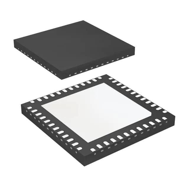
1 GHz clock synthesis — output flexibility
The LMK03328RHST: The PLL core generates up to 1 GHz on the outputs, covering the reference clock rates for most high-speed SerDes, FPGA transceivers, and Ethernet PHYs. The 2:8 input-to-output ratio means two reference inputs feed eight synthesised outputs — enough to distribute a clean clock to multiple ASICs or line cards without external fan-out buffers. Output format is configurable across CML, HCSL, LVCMOS, LVDS, and LVPECL. A single device can drive a PCIe reference (HCSL), a backplane clock (LVDS), and a local FPGA fabric clock (LVCMOS) from the same die, reducing the component count in a mixed-signal timing tree. The PLL includes a bypass mode, which lets the input clock pass through to the outputs without phase-locked-loop processing. This is useful for jitter-sensitive paths where the PLL's own phase noise would degrade the signal, or for test modes where a clean reference is needed directly.
Supply and temperature — board-level fit
The wide range also allows the same BOM to serve multiple voltage domains across different board spins.