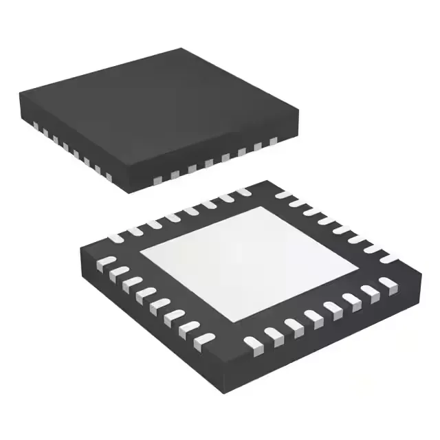
Texas Instruments LMK00334RTVR — Clock & Timing ICs

TI LMK00334RTVR PCIe/SATA Clock Fanout Buffer, 400 MHz, 3:5

MPNLMK00334RTVR
Active

Texas Instruments LMK00334RTVR, 3:5 differential fanout buffer, 400 MHz max frequency, accepts CML/HCSL/HSTL/LVDS/LVPECL/SSTL/Crystal inputs, HCSL/LVCMOS outputs, 3.15V-3.45V supply, -40°C to 85°C, 32-WQFN.

$2.9600Ref. price · indicative, final on quote
Sourced new & surplus through independent channelsAuthenticity-screened · ESD-safe packingListing updated Aug 2026

Specifications

LMK00334RTVR specifications
ParameterValue
MountingSurface Mount
Voltage3.15V ~ 3.45V
Frequency400MHz
Operating temperature-40°C~85°C
PLLNo
InputCML, HCSL, HSTL, LVDS, LVPECL, SSTL, Crystal
OutputHCSL, LVCMOS
PackageTape & Reel (TR); Cut Tape (CT)
Main purposePCI Express (PCIe), SATA CPU
Case32-WFQFN Exposed Pad
Number of circuits1
Ratio - Input:Output3:5
Differential - Input:OutputYes/Yes

Product details

400 MHz fanout — the PCIe Gen3 reference clock workhorse

The LMK00334RTVR is a 3:5 differential fanout buffer from Texas Instruments designed for PCI Express and SATA CPU reference clock distribution. It accepts seven input standards — CML, HCSL, HSTL, LVDS, LVPECL, SSTL, and Crystal — and outputs HCSL or LVCMOS. The 400 MHz maximum frequency covers PCIe Gen3 (100 MHz or 125 MHz reference clocks) with margin for Gen4 or Gen5 if the system stays within the 400 MHz ceiling.

Input flexibility — one buffer, seven clock standards

The 3:1 input mux accepts CML, HCSL, HSTL, LVDS, LVPECL, SSTL, and Crystal inputs. That means a single BOM line handles the reference clock fanout for a PCIe root complex (HCSL or LVDS), a SATA controller (CML or LVPECL), and an FPGA transceiver bank (HSTL or SSTL) — no need for separate level translators or dedicated fanout buffers per standard. The differential input-to-output path is fully differential (Yes/Yes), so the buffer preserves the signal integrity of the incoming clock through the fanout tree. The single-ended Crystal input is available for a local oscillator, but the output remains HCSL or LVCMOS — the part does not include a PLL for frequency synthesis.

Supply and temperature — the industrial clock-tree envelope

The 3.15V to 3.45V supply range is a 3.3V nominal rail with ±4.5% tolerance. Staying inside that window matters: the buffer's PSRR is specified at 3.3V, and a rail outside the tolerance injects supply noise that adds jitter to the output clocks.

Package and footprint — 32-WQFN with exposed pad

Frequently asked questions

What are the input and output types supported by LMK00334RTVR?

The outputs are HCSL or LVCMOS. The part does not include a PLL, so it buffers the incoming clock without frequency synthesis or jitter cleaning.

Is LMK00334RTVR RoHS compliant and lead-free?

Confirm the specific date-code compliance certificate with your distributor at order time.

Is LMK00334RTVR compatible with PCIe Gen3?

Yes. PCIe Gen3 uses a 100 MHz or 125 MHz reference clock, and the LMK00334RTVR is rated for 400 MHz maximum frequency. The buffer's HCSL output is the standard PCIe reference clock format, and the differential input path accepts the HCSL or LVDS output from the PCIe root complex.