Clock distribution hub for high-speed serial links
The Texas Instruments LMK00304SQX/NOPB is a 3.1 GHz fanout buffer, multiplexer, and translator that sits at the centre of a clock tree distributing reference clocks to multiple high-speed serial links. It accepts one of three input sources — CML, HCSL, HSTL, LVDS, LVPECL, SSTL, or a crystal — and fans out to five outputs in HCSL, LVCMOS, LVDS, or LVPECL formats, with all differential paths maintained end-to-end.
3.1 GHz bandwidth and IO standard flexibility
The 3.1 GHz maximum frequency covers the full range of PCIe Gen 1 through Gen 5 reference clocks, 10GbE, and 100G/400G line-card timing. The 3:5 input-to-output ratio means three selectable clock sources feed five output banks — useful for redundant clock architectures where a primary and backup oscillator share the same buffer. Differential input and output paths (Yes/Yes per the spec) preserve signal integrity through the buffer; the part translates between input and output standards, so a CML source can drive LVDS loads without an external level shifter.
32-WQFN package and board integration
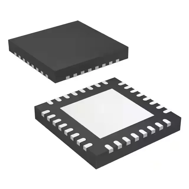
The 32-WFQFN exposed-pad package (5 mm × 5 mm body) requires a thermal pad on the PCB to draw heat from the die. The supplier device package is 32-WQFN (5x5) — the same footprint as the standard 32-QFN, but the exposed pad dimensions and via pattern should match the TI recommended land pattern in the datasheet for thermal and electrical performance.