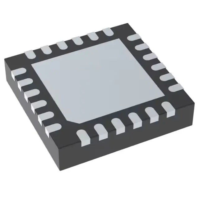
What this clock buffer does on the board
The LMK00105SQX/NOPB is a three-in-one clock-tree part: a fanout buffer, a signal multiplexer, and a level translator in a single 24-WQFN package. It takes in one of seven differential or single-ended input formats — HCSL, LVCMOS, LVDS, LVPECL, LVTTL, SSTL, or a crystal — and outputs five copies of that clock in LVCMOS logic levels. The 2:5 input-to-output ratio means you can select between two clock sources (the mux function) and distribute the chosen clock to five downstream loads without adding a separate mux and fanout buffer. The differential inputs accept a clean differential clock while the single-ended outputs drive standard CMOS logic — no external level-shifting resistors needed between the clock source and the FPGA or ASIC bank.
Frequency ceiling and signal integrity
Rated to 200 MHz maximum, this buffer handles the common clock rates for Gigabit Ethernet, PCIe Gen 1/2 reference clocks, and most FPGA fabric clocks. The differential input path preserves signal integrity at the higher end of the band — the HCSL or LVDS inputs reject common-mode noise picked up on the board trace between the oscillator and this buffer.
Package reality for the rework bench
Will it survive hot air? Yes — the QFN body is small enough that a preheat plate at 150 °C followed by a hot-air nozzle at 300 °C lifts the part cleanly without lifting adjacent passives, as long as the board has adequate copper soak under the pad. The 24-WQFN (4x4) supplier device package matches the industry-standard QFN footprint, so replacement parts from the same reel reflow back without pad realignment.
Active lifecycle and procurement posture
The base product number LMK00105 covers the whole family; the /NOPB suffix indicates lead-free (RoHS-compliant) plating on the terminations.