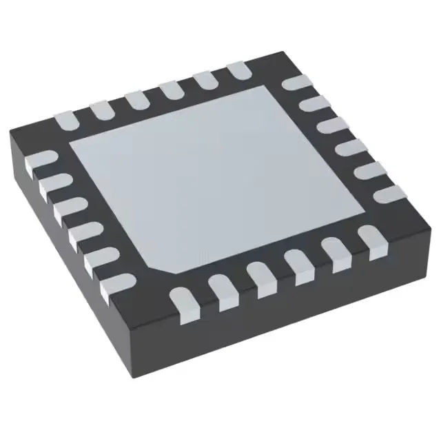
Clock distribution and signal translation in one package
The Texas Instruments LMK00105SQE/NOPB combines a fanout buffer, multiplexer, and level translator in a single 24-WFQFN package — a single IC that cleans up a clock tree by accepting differential or single-ended inputs and delivering LVCMOS outputs to multiple loads. Rated for 200 MHz maximum frequency, it handles the common clock rates found in Ethernet PHYs, FPGAs, and baseband processors without adding jitter beyond the device's own additive phase noise floor. The 2:5 input-to-output ratio means two selectable clock sources feed five output branches — useful for redundancy switching or distributing a clean reference across a multi-rail board.
What the input flexibility means for your BOM
The LMK00105SQE/NOPB accepts HCSL, LVCMOS, LVDS, LVPECL, LVTTL, SSTL, and crystal inputs — covering nearly every differential and single-ended standard used in high-speed digital systems. One BOM line replaces a dedicated translator and a separate fanout buffer. The differential input path (Yes/No flag) means the device can cleanly buffer a differential pair like LVDS or LVPECL and output single-ended LVCMOS — no external termination network needed beyond the standard 100-ohm differential termination.
The 24-WFQFN with exposed pad (4x4 mm body) requires a thermal land on the PCB to pull heat from the die — the datasheet's recommended PCB layout pattern should be followed for the pad's solder paste stencil aperture to avoid voids under the package. Surface-mount assembly with the 24-WQFN (4x4) supplier package means standard reflow profiles for QFN packages apply — the exposed pad's solder joint is the primary thermal path, so the board's copper pour under the pad should connect to the ground plane with at least nine thermal vias.