What this P-channel load switch does on your rail
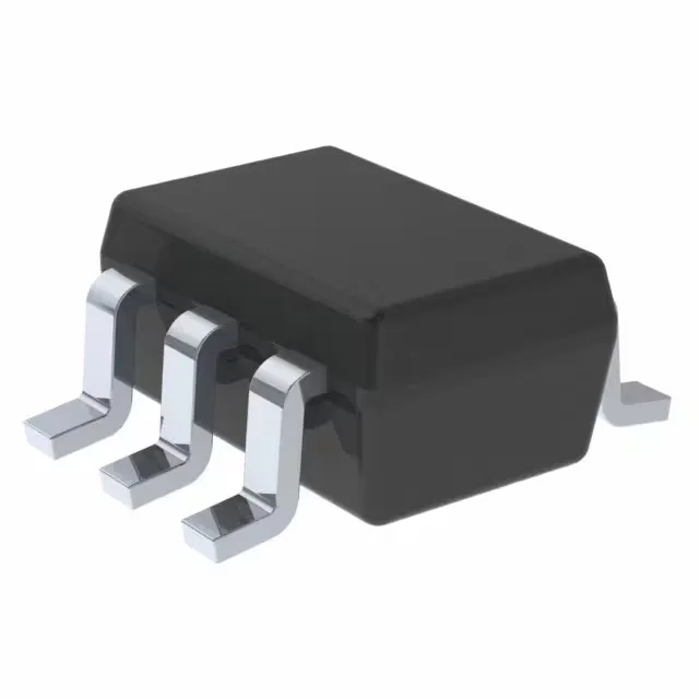
The LM66100DCKR: The P-channel FET sits on the high side, so no external charge pump or boost circuit is needed — just the input rail and an enable signal.
Supply range and load budget — what fits
At 1.5 A max output, this switch is sized for downstream loads like sensor modules, RF front-ends, or small FPGA core rails — not a main power bus.
Turn-on and turn-off timing for sequencing
The 27 µs turn-on delay is deliberate — it limits inrush current into a capacitive load. The 2 µs turn-off is fast enough to isolate a faulted rail before the supply droops. If your design requires a specific power-up sequence between multiple rails, this asymmetric delay matters: the load gets power slowly but drops quickly on a fault or disable.
Package and footprint — SC-70-6
The SC-70-6 (SOT-363) body is 2.0 mm × 1.25 mm, with 0.65 mm pin pitch. A 2-layer board with minimal copper pours will hit the thermal ceiling faster than a 4-layer with a solid ground plane.