Texas Instruments LM5112MYX/NOPB — Analog & Data Acquisition

LM5112MYX/NOPB Low-Side Gate Driver, 3A/7A Peak, Active

MPNLM5112MYX/NOPB
End of Life

Texas Instruments LM5112MYX/NOPB, single low-side gate driver for N-Channel MOSFETs, 3.5V~14V supply, 3A source / 7A sink peak output, 14ns/12ns rise/fall, inverting and non-inverting inputs, -40°C to 125°C, 8-HVSSOP package, Tape & Reel.

$1.59Ref. price · indicative, final on quote
Packaging8-TSSOP, 8-MSOP (0.118", 3.00mm Width) Exposed Pad
StockContact for availability
MOQ1 pcs
  • 100% new & originalTraceable channels only — no refurbs, no pulls, no remarked parts.
  • Date & lot codes on quoteStated per line before you commit; label photos on request.
  • MSL-compliant ESD packingMoisture-sealed bags with indicator cards; reels photo-verified.
  • PayPal buyer protectionPay by T/T, PayPal or Payoneer — card payments covered end to end.

Specifications

LM5112MYX/NOPB Technical Specifications
ParameterValue
Gate typeN-Channel MOSFET
Input typeInverting, Non-Inverting
Channel typeSingle
Mounting typeSurface Mount
Voltage3.5V ~ 14V
Logic voltage - VIL, VIH0.8V, 2.3V
Current - peak output (Source, sink)3A, 7A
Operating temperature-40°C ~ 125°C (TJ)
PackageTape & Reel (TR); Cut Tape (CT)
Case8-TSSOP, 8-MSOP (0.118\", 3.00mm Width) Exposed Pad
Number of drivers1
Driven configurationLow-Side
Rise (Fall time)14ns, 12ns

Product details

Low-side gate driver for N-channel MOSFETs

The Texas Instruments LM5112MYX/NOPB is a single-channel low-side gate driver designed to drive N-Channel MOSFETs. It accepts both inverting and non-inverting input logic, giving you flexibility in how the PWM signal from the controller connects. The supply range runs from 3.5V to 14V, which covers most common control rails — 5V and 12V logic alike. Peak output current is rated at 3A source and 7A sink, so it can charge and discharge the gate capacitance quickly enough to keep switching losses under control in a typical DC-DC converter or synchronous rectifier stage. Rise and fall times are 14 ns and 12 ns respectively, putting this in the fast-switching class for a single low-side driver. The part is housed in an 8-HVSSOP package with an exposed pad for thermal relief, and it operates across the full industrial temperature range of -40°C to 125°C.

Package and mounting

Peak output is 3A source and 7A sink. Rise time is 14 ns and fall time is 12 ns.

Package and mounting

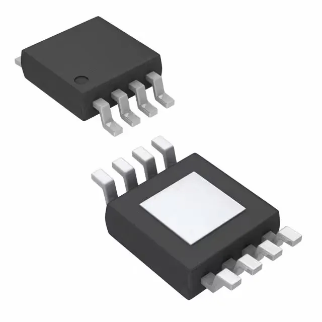
The LM5112MYX/NOPB comes in an 8-HVSSOP package — that is the 3 mm × 3 mm body with an exposed pad underneath. The pad needs a thermal via or a copper pour on the PCB to pull heat out of the die. Without it, the junction temperature rises faster than the -40°C to 125°C rating suggests, especially when driving a high gate charge at high frequency. The part is surface-mount only; no through-hole variant exists. It ships on Tape & Reel, which is the standard for automated pick-and-place.

Lifecycle and sourcing

The LM5112MYX/NOPB is listed as Active with ROHS3 compliance. You can qualify it into a new BOM without worrying about a sudden EOL.

Frequently asked questions

What is the difference between LM5112MYX and LM5112MYX/NOPB?

The LM5112MYX/NOPB is the ROHS3-compliant version of the base LM5112MYX. The electrical specifications — supply range, peak output current, rise/fall times — are identical. The /NOPB suffix is Texas Instruments' designation for lead-free / RoHS-compliant packaging.

What is the typical rise time for the LM5112MYX/NOPB?

Typical rise time is 14 ns, and typical fall time is 12 ns. These are the times the output takes to swing from 10% to 90% of the final value under the test conditions specified in the datasheet.