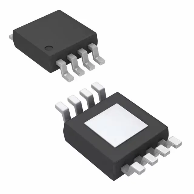
Texas Instruments LM5112MY/NOPB — Analog & Data Acquisition

LM5112MY/NOPB Low-Side Gate Driver, 3A/7A Peak, 8-HVSSOP

MPNLM5112MY/NOPB
End of Life

Texas Instruments LM5112MY/NOPB, single low-side gate driver for N-Channel MOSFETs, 3A source / 7A sink peak output, 3.5V–14V supply, 14ns/12ns rise/fall, 8-HVSSOP exposed-pad package, -40°C to 125°C.

$1.91Ref. price · indicative, final on quote
Packaging8-TSSOP, 8-MSOP (0.118", 3.00mm Width) Exposed Pad
StockContact for availability
MOQ1 pcs
  • 100% new & originalTraceable channels only — no refurbs, no pulls, no remarked parts.
  • Date & lot codes on quoteStated per line before you commit; label photos on request.
  • MSL-compliant ESD packingMoisture-sealed bags with indicator cards; reels photo-verified.
  • PayPal buyer protectionPay by T/T, PayPal or Payoneer — card payments covered end to end.

Specifications

LM5112MY/NOPB Technical Specifications
ParameterValue
Gate typeN-Channel MOSFET
Input typeInverting, Non-Inverting
Channel typeSingle
Mounting typeSurface Mount
Voltage3.5V ~ 14V
Logic voltage - VIL, VIH0.8V, 2.3V
Current - peak output (Source, sink)3A, 7A
Operating temperature-40°C ~ 125°C (TJ)
PackageTape & Reel (TR); Cut Tape (CT)
Case8-TSSOP, 8-MSOP (0.118\", 3.00mm Width) Exposed Pad
Number of drivers1
Driven configurationLow-Side
Rise (Fall time)14ns, 12ns

Product details

Single low-side gate driver with 3A source, 7A sink

The Texas Instruments LM5112MY/NOPB is a single-channel low-side gate driver designed to drive N-channel MOSFETs. Its 3A peak source and 7A peak sink current capability — paired with 14 ns typical rise and 12 ns typical fall times — delivers the gate charge needed for fast switching in synchronous rectifiers, DC-DC converters, and motor-drive output stages. The input accepts both inverting and non-inverting logic, so a single part covers both polarity requirements from the controller without an external inverter gate.

Supply rail and logic thresholds

Operating supply range runs from 3.5 V to 14 V. The VIL/VIH thresholds are set at 0.8 V and 2.3 V.

Package thermal path — the exposed pad matters

The 8-HVSSOP package (3.00 mm width, exposed pad) is the same footprint as a standard 8-MSOP but with a thermal pad underneath. For sustained operation near the 3 A / 7 A peak ratings, that pad must be soldered to a copper plane on the PCB — the datasheet's thermal resistance figures assume a proper ground-plane connection. Without it, junction temperature climbs faster than the -40°C to 125°C rating suggests. The part is surface-mount only; no through-hole variant exists in this family.

Lifecycle and sourcing position

Status is Active per the manufacturer — no end-of-life notice, no last-time-buy clock running. ROHS3 compliant.

Frequently asked questions

What is the peak source and sink current of LM5112MY/NOPB?

Peak output current is 3 A source and 7 A sink. That asymmetric ratio is intentional — the higher sink current pulls the MOSFET gate down faster than it charges it, which helps control the turn-off di/dt and reduces shoot-through margin in half-bridge stages.

Can LM5112MY/NOPB be used with both inverting and non-inverting inputs?

Yes, the input accepts both inverting and non-inverting logic. A single part covers either polarity requirement from the PWM controller without adding an external inverter gate.

What are the alternatives or equivalents for LM5112MY/NOPB?

The closest functional peer in TI's portfolio is the LM5106MM/NOPB, a half-bridge driver with two outputs and 1.2 A switching current. It is not a pin-for-pin substitute — the LM5106 adds a bootstrap diode for high-side drive and changes the package to an 8-MSOP-PowerPad. If you need a single low-side driver, the LM5112MY/NOPB is the correct part; the LM5106 serves a different topology.