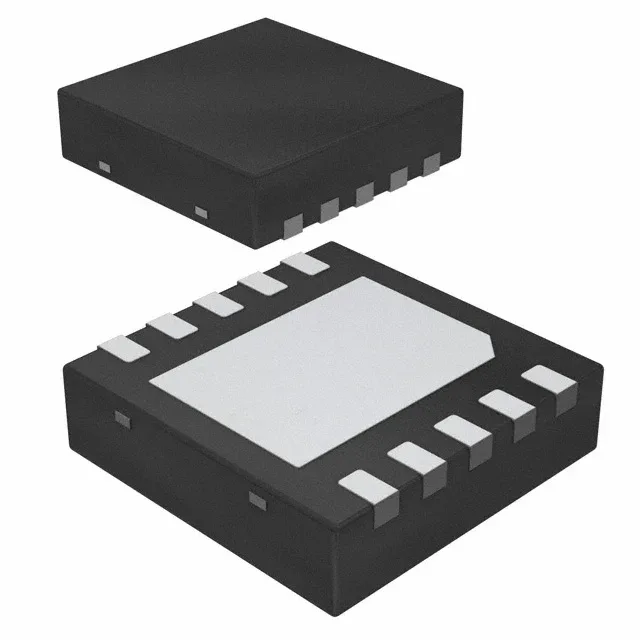
Dual low-side gate driver for N-channel power stages
The Texas Instruments LM5110-2SD/NOPB is a dual, independent low-side gate driver designed to drive N-channel MOSFETs. It delivers a peak output of 3 A source and 5 A sink, which is enough current to charge and discharge the gate capacitance of medium-power MOSFETs quickly, reducing switching losses in the transition region. Each of the two channels operates independently with an inverting input, and the supply voltage range of 3.5 V to 14 V covers the common gate-drive rails from a 5 V logic supply up to a 12 V bias for standard MOSFET thresholds.
Switching speed and thermal envelope
Typical rise and fall times of 14 ns and 12 ns respectively, driving a 1 nF load, mean the driver can switch a MOSFET gate fast enough for converter frequencies in the hundreds of kilohertz. The 14 ns rise time into a typical gate charge keeps the Miller plateau brief, which directly reduces the time the MOSFET spends in the linear region during each transition. Rated for operation from -40°C to +125°C junction temperature, the driver suits industrial and automotive environments where the ambient temperature inside the enclosure can exceed 85°C. The 10-WSON package with an exposed pad (4x4 mm) needs a thermal land on the PCB to pull heat out of the die; without it, the junction temperature rise at full switching frequency may exceed the 125°C limit.
Logic interface and supply rail compatibility
A 3.3 V microcontroller output above 2.2 V is read as a logic high; a 5 V TTL output below 0.8 V is a logic low. No external level shifting is needed for these common logic rails.