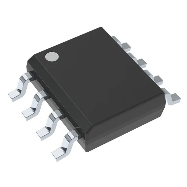
Dual low-side gate driver for synchronous buck and half-bridge stages
The LM5110-1MX/NOPB is a dual low-side gate driver from Texas Instruments designed to drive N-channel MOSFETs in power-converter and motor-drive stages. Each of the two independent channels delivers 3 A peak source and 5 A peak sink current, giving it the drive strength to charge and discharge the gate capacitance of a pair of paralleled TO-220 MOSFETs or a single large-die device in a half-bridge leg. The non-inverting input logic means the output follows the input without polarity inversion — useful when the PWM controller already provides the correct phase. Supply voltage spans 3.5 V to 14 V, so the gate drive amplitude can be set to 10 V for standard MOSFETs or dropped to 5 V for logic-level devices, as long as the controller's output high level clears the 2.2 V VIH threshold.
Switching speed and thermal budget
Rise and fall times are 14 ns and 12 ns typical into a 1 nF load — the actual transition time on your board depends on the total gate charge of the MOSFET and the layout's parasitic inductance. A 14 ns rise into a 10 nC gate (typical for a 40 A-rated TO-220 FET) means the driver delivers roughly 0.7 A average during the transition, well within the 3 A peak capability, so the limiting factor is the loop inductance, not the driver's output stage.
Board-level integration and supply posture
The independent channel architecture means the two outputs can drive separate MOSFETs in an interleaved converter or be paralleled for higher peak current by tying the inputs together — though the datasheet's recommended layout should be followed to avoid shoot-through during the overlap window.