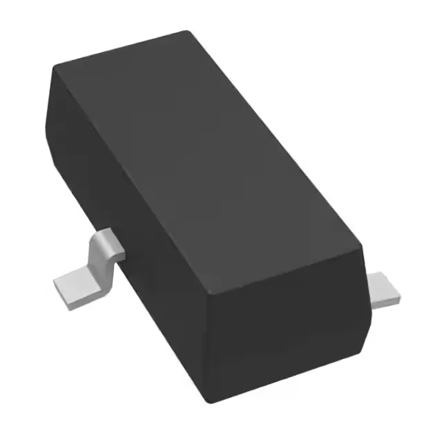
Adjustable shunt reference — 1.233 V to 10 V in a SOT-23-3
It is a two-terminal device — the shunt topology means it behaves like a Zener diode but with a ±1% initial tolerance and a 150 ppm/°C temperature coefficient that holds the voltage tighter than a standard Zener over temperature. The SOT-23-3 package keeps the footprint small — three pads, no thermal pad needed — which suits dense mixed-signal boards where an ADC or DAC needs a clean bias rail and board area is tight.
Output range and bias resistor sizing
The minimum output is 1.233 V (the internal bandgap voltage); the maximum is 10 V, limited by the shunt architecture. To set an intermediate voltage, pick R1 and R2 per the standard shunt-reference formula: Vout = 1.233 V × (1 + R1/R2). The 70 µA minimum cathode current means the bias resistor from the supply to the reference's cathode must pass at least 70 µA plus the load current at all times — undersize the resistor and the reference drops out of regulation. The 12 mA output current ceiling limits how many downstream loads the reference can drive. For a single ADC reference input drawing 200 µA, the headroom is ample; for a multi-channel SAR array or a precision DAC reference input, sum the loads and stay under 12 mA total.
Noise and temperature drift for precision loops
The 20 µVrms noise over the 10 Hz to 10 kHz band is low enough for 12-bit systems but may need additional filtering for 16-bit or higher-resolution converters where the noise floor must sit below 1 LSB. The 150 ppm/°C temperature coefficient means the output shifts about 0.15 mV per degree at a 1.233 V setpoint — acceptable for industrial temperature swings but not for metrology-grade references.