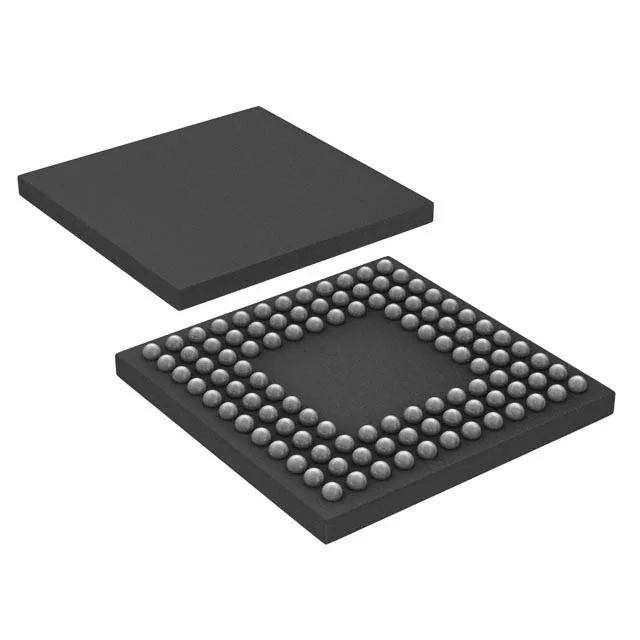
It runs at 80 MHz and packs 384 KB of Flash program memory alongside 96 KB of SRAM, which is enough for a real-time control stack plus a TCP/IP or CANopen protocol layer without external memory. The core is a single-cycle multiply Cortex-M3 with a 32-bit bus matrix, so the 80 MHz clock delivers deterministic interrupt response for time-critical control loops. On-chip peripherals include a 16-channel 12-bit ADC, PWM outputs, quadrature encoder interface (QEI) for motor position feedback, and a DMA controller that can move data between Ethernet, USB, and serial buffers without CPU intervention. The internal oscillator trims to within 1% accuracy, though an external crystal is still the right choice for CAN or Ethernet timing where the spec demands ±0.5% tolerance.
Texas Instruments has ended production, with no last-time-buy window currently open. Any migration will require a firmware port and re-validation of the board-level timing, not just a re-spin of the BOM line.
80 MHz Cortex-M3 — what the speed rating delivers
The 80 MHz core clock is the single performance anchor for this part. At this speed the Cortex-M3 executes most single-cycle instructions in 12.5 ns, which means a PID loop with 10 µs update rate has roughly 800 instructions per cycle — comfortable for a motor control or power-conversion algorithm. The Flash memory uses a prefetch buffer to avoid wait-state penalties at 80 MHz, so tight loops in the control ISR run at full speed without stalling on instruction fetches. Compare this to the 50 MHz variants in the same Stellaris family: the 80 MHz part gives a 60% throughput headroom for protocol processing (Ethernet frame forwarding, CAN message filtering) on top of the control workload. If your application already runs at 50 MHz with 70% CPU load, this part buys margin for future feature additions without a core architecture change.
BGA footprint and board-level considerations
The 108-ball BGA (10x10 mm array, 0.8 mm pitch) is a compact package that saves board area versus a 100-pin LQFP, but it demands at least a 4-layer PCB with buried vias for fanout. The ball map is a 12x12 grid with the center rows depopulated, so routing the inner balls to the outer perimeter requires via-in-pad or microvia techniques on high-density designs. The core supply is 1.235 V to 1.365 V, a narrow range that needs a dedicated LDO or switching regulator with tight regulation. The I/O supply is separate (3.3 V typical) and powers the 65 GPIOs plus the Ethernet PHY and USB transceiver. Decoupling the 1.3 V core rail with a 10 µF ceramic plus 0.1 µF per supply pin pair is the baseline; the Ethernet PHY's analog supply needs its own LC filter to keep switching noise out of the transmit signal.