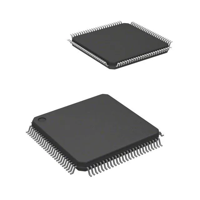
The 256 KB Flash is organized as 256K x 8 bits, enough for a TCP/IP stack (lwIP or uIP), an RTOS kernel, and application code. The 64 KB SRAM must accommodate two Ethernet frame buffers (about 3 KB each for a standard 1518-byte frame) plus stack and heap. If the application uses a web server with multiple simultaneous connections, the SRAM budget tightens — plan the buffer pool size early in firmware design.
Supply rail: 2.5 V nominal — plan the regulator
This is not a 3.3 V part; the board needs a dedicated 2.5 V LDO or buck converter. Any 3.3 V peripherals on the same PCB will require level shifters on the I/O lines. The 38 GPIOs are 2.5 V tolerant, not 5 V — check the absolute maximums before connecting to legacy 5 V logic.
100-LQFP footprint — layout notes for Ethernet
The integrated Ethernet PHY differential pairs (TXP/TXN, RXP/RXN) must be routed with controlled impedance (100 Ω differential) and kept away from the 50 MHz crystal and switching regulator. The 14x14 mm body fits on a two-layer board, but a four-layer stack-up with a ground plane makes the Ethernet signal integrity much easier to close.