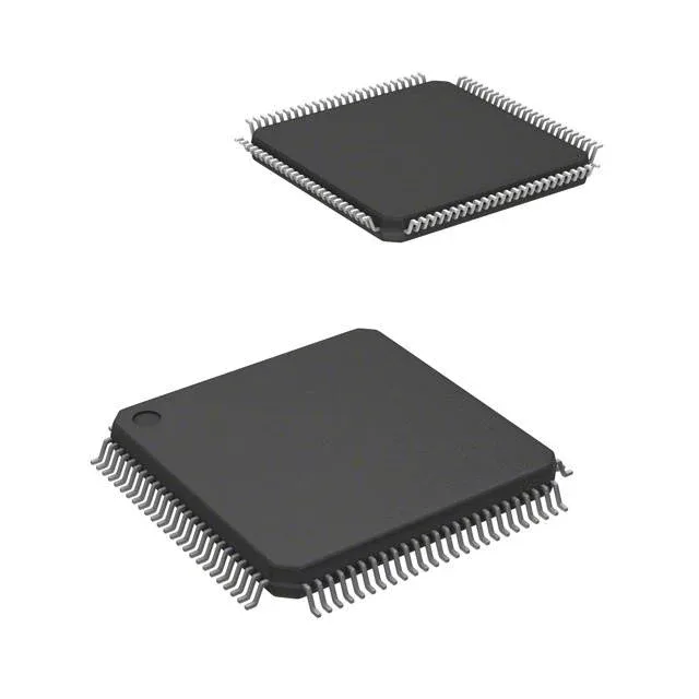
What this part is and what it brings to the board
The LM3S5B91-IQC80-B1: It integrates 256 KB of flash and 96 KB of SRAM on-chip — the flash holds the application image and bootloader, while the SRAM gives the stack and heap enough room for real-time control loops without external memory. The 100-pin LQFP package (14x14 mm body) exposes 72 general-purpose I/O lines. The peripheral set includes a 16-channel 10-bit ADC, multiple serial interfaces (CAN, I²C, SPI, UART, USB OTG), and motion-control blocks like PWM and QEI — a fit for industrial drives, sensor hubs, or human-machine interface panels that need a single-chip control core.
Memory and peripheral headroom for the firmware engineer
256 KB of on-chip flash (256K x 8) leaves room for a moderate application stack plus a RTOS kernel. The 96 KB SRAM (96K x 8) is split across the core and peripheral DMA — enough for double-buffered frame data in a display application or for holding a large parameter table without paging. The connectivity block covers CANbus, USB OTG, and multiple UART/USART channels — the CAN interface suits industrial automation backbones, while USB OTG lets the MCU act as either host or device for field-upgrade or data-logging roles. On-chip peripherals include a brown-out detect, POR, DMA, I²S audio interface, PWM, and a watchdog timer. The internal oscillator means the part can run without an external crystal for basic clocking, though the USB block will require an accurate external source for full-speed operation.
Lifecycle reality and sourcing path
Sourcing for this MCU goes through independent distribution and surplus channels. Each unit's date-code and marking are verified against TI's factory records before shipment — the laser etch and package traceability are checked for consistency. The 100-LQFP (14x14 mm) footprint is a standard JEDEC outline — replacement parts in the same package family exist, but a pin-compatible drop-in is not guaranteed without reviewing the full pinout and peripheral map.