80 MHz Cortex-M3 with USB OTG and CAN — what this part was designed for
The 72 general-purpose I/O lines and 16-channel 10-bit ADC handle local sensor and actuator interfaces.
There is no listed successor or pin-compatible replacement in the official record. Buyers should verify date codes and request trace documentation, particularly for moisture-sensitive 100-LQFP packages that may have been in storage beyond their floor-life window.
The 80 MHz core clock is the headline performance spec. On a Cortex-M3 with a single-cycle multiply and a 3-stage pipeline, 80 MHz delivers roughly 80 DMIPS, which is enough for real-time control loops (motor FOC, PID at 10–20 kHz update rates) and moderate protocol processing (USB bulk transfers, CAN message handling). The flash wait state at 80 MHz needs to be set to at least 1 wait state per the reference manual — running at full speed with zero wait states will cause hard faults on the first branch. The 64 KB SRAM is sufficient for a single USB buffer and a few CAN message objects without external memory, but designs with large frame buffers or data logging will need the EBI/EMI interface for external SRAM or FRAM.
Package and supply — what to check before layout
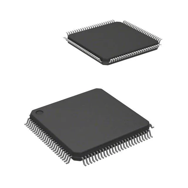
The LM3S5791-IQC80-C3T is supplied in a 100-LQFP package (14x14 mm body) with a 0.5 mm pitch. The core logic runs from a 1.08 V to 1.32 V supply, while the I/O bank is powered separately — the exact I/O voltage range is not listed in this record, so the datasheet must be consulted for the VDDIO pin voltage. The 100-LQFP has an exposed pad (thermal pad) on the bottom; a via stitch to a ground plane is required to keep junction temperature under control at high I/O activity and 80 MHz switching.