What the 80 MHz core and memory map mean for the firmware budget
The LM3S5651-IBZ80-C5T runs an ARM Cortex-M3 core at 80 MHz — the 1.25 MIPS/MHz ceiling gives 100 MIPS through the single-cycle multiply and hardware divide, but the flash-wait state profile at this clock determines the actual throughput. With 128 KB of program flash and 32 KB of SRAM, the bootloader and HAL footprint need to stay under 16 KB to leave room for the application stack and a moderate RTOS heap. The 32-bit single-core architecture and internal oscillator mean the part boots without an external crystal — the clock tree starts from the internal RC and can be switched to a PLL for the full 80 MHz.
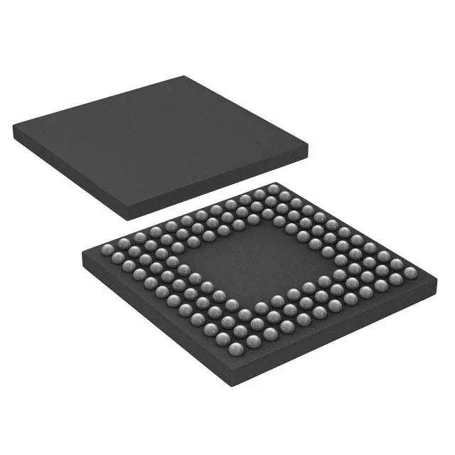
The part packs CAN, USB OTG, I²C, SPI, SSI, UART/USART, IrDA, LIN, and Microwire — enough to bridge a CANopen fieldbus to a USB debug port while logging sensor data over SPI to an external ADC. The 16-channel 10-bit ADC samples at the rate the application scheduler allows; the QEI peripheral decodes quadrature encoder pulses without CPU intervention. With 67 I/O lines in a 108-ball BGA (10x10 mm), the fan-out on a four-layer board is manageable — the 0.80 mm ball pitch leaves room for a via-in-pad escape on the inner layers.
Texas Instruments lists the LM3S5651-IBZ80-C5T as obsolete.