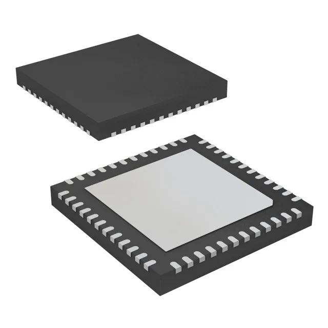
25 MHz Cortex-M3 with 16 KB flash — what fits in that footprint
The LM3S308-EGZ25-C2: That is a tight memory budget — enough for a single-loop control task or a UART-to-SPI bridge, but not for a full RTOS plus application stack. The 4 KB SRAM (organized as 4K x 8) leaves around 2.5 KB after the vector table and minimal HAL, so every global buffer counts. The part is in the Stellaris ARM Cortex-M3S 300 series, TI's first-generation Cortex-M3 family. It uses the ARMv7-M architecture with a single-cycle multiply and a 12-cycle divide — no FPU, no MPU. The 25 MHz ceiling is set by the internal oscillator; the device can also run from an external crystal or a PLL-locked source, though the PLL is not available on all package variants.
Industrial temp grade and on-chip peripherals
On-chip peripherals include a PWM module, a watchdog timer, and an 8-channel 10-bit ADC. The connectivity block supports I2C, Microwire, SPI, SSI, and UART/USART — enough for a sensor hub or a simple motor controller. The 28 general-purpose I/O lines are 5 V tolerant on most pins, which simplifies level translation when interfacing to legacy 5 V logic.
48-VQFN package — thermal pad and layout notes
The device comes in a 48-VFQFN exposed pad package (7x7 mm body, 0.5 mm pitch). Surface-mount assembly with a tray handling option — the package is not moisture-sensitive above MSL 3 per JEDEC, but a bake-out before reflow is recommended if the shelf life has been exceeded. The 0.5 mm pitch demands a solder paste stencil aperture of about 0.25 mm width for the perimeter pads; the center pad needs a grid of small apertures to avoid voiding.
The base product number is LM3S308 — the suffix -EGZ25-C2 encodes the package (48-VQFN), temperature range (industrial), and speed grade (25 MHz). When ordering, verify the full order code against the BOM position; the -C2 suffix indicates the latest silicon revision, which incorporates errata fixes from earlier stepping levels.