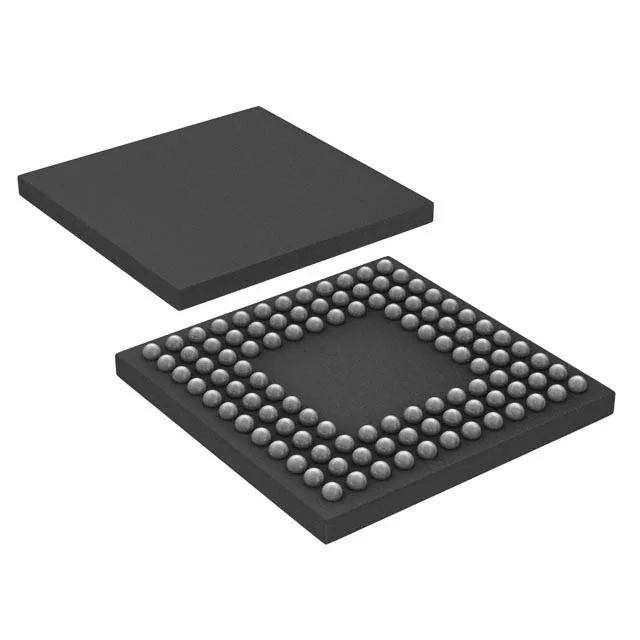
Core architecture and memory map
The LM3S2U93-IBZ80-A2: Built around the ARM Cortex-M3 core at 80 MHz, this 32-bit single-core MCU delivers the deterministic interrupt handling and Thumb-2 instruction set typical of the M3 family. On-chip program memory is 384 KB of flash, paired with 96 KB of SRAM — the 96K x 8 entry maps to 96 KB of byte-addressable RAM. For a Cortex-M3 class device, the 1:4 flash-to-RAM ratio is generous, suiting applications that keep a moderate-sized frame buffer or communication stack in SRAM.
The peripheral list includes CANbus, EBI/EMI, I²C, IrDA, Microwire, QEI, SPI, SSI, and UART/USART — a broad mix that covers industrial fieldbus (CAN), external memory expansion (EBI/EMI), and sensor interfaces (SPI, I²C). The 16-channel 10-bit ADC provides analog acquisition without an external converter. On-chip peripherals also include brown-out detect/reset, DMA, I²S, POR, PWM, and WDT. The 67 I/O lines give enough headroom for a parallel display or memory bus alongside GPIO.
Package, power, and temperature grade
Housed in a 108-LFBGA package with a supplier device package designation of 108-BGA (10x10). The 10x10 mm body with a 0.80 mm ball pitch is a standard footprint for this density — four-layer board with via-in-pad is typical for fan-out.