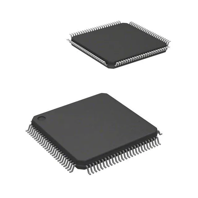
Package and board-fit for the 100-LQFP
The LM3S2412-EQC25-A2 comes in a 100-LQFP package with a 14x14 mm body. The 0.50 mm pitch demands a controlled impedance stack-up on the outer rows for signal integrity, and a 4-layer board is typical for fan-out of the 49 I/O plus supply and ground pins.
Compute and memory for the firmware budget
The ARM Cortex-M3 core runs at 25 MHz with a single-cycle multiply and hardware divide — enough for moderate control loops and protocol handling without an external coprocessor. 96 KB of on-chip Flash holds the application code and bootloader; 32 KB of SRAM leaves headroom for stack, heap, and data buffers in a typical sensor or actuator node. Program memory is Flash type — field firmware updates are viable over the CAN or UART bootloader, but the 100k erase/write cycle endurance (typical for this process) means wear-leveling is not needed for most product lifetimes.
Peripheral integration for control and connectivity
The part integrates CAN, I²C, SPI, SSI, UART, and IrDA interfaces — enough to bridge a CAN-based fieldbus to a local sensor bus or debug UART without external bridge chips. On-chip peripherals include a 3-channel 10-bit ADC, PWM outputs, brown-out detect, POR, and a watchdog timer — covering the basic analog sampling and supervisory functions for an embedded control board. 49 general-purpose I/O pins are available, multiplexed with the peripheral functions — enough for a modest keypad, display, and sensor interface without an external GPIO expander.
Lifecycle reality and sourcing for the BOM line
For a BOM line requiring an active-production alternative, a parametric search within the Stellaris family for a Cortex-M3 at a similar speed and memory tier is the next step — but expect a different package and pinout, requiring a board spin.