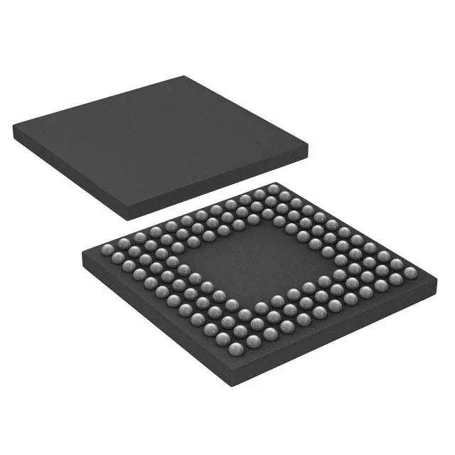
80 MHz ARM Cortex-M3 in a 108-BGA — what this MCU delivers
Connectivity spans I²C, IrDA, Microwire, QEI, SPI, SSI, and UART/USART. The integrated 16-channel 10-bit ADC and internal oscillator reduce external component count.
64 KB Flash and 24K x 8 RAM — firmware and data headroom
The 64 KB Flash (64K x 8) is the program store; a firmware image that fits within this boundary can be field-upgraded via the internal bootloader or SWD. The 24K x 8 SRAM provides working space for stack, heap, and DMA buffers. For a control application with moderate data logging or communication buffering, this RAM allocation is adequate — but a design that needs large look-up tables or multiple frame buffers should verify headroom early. The Flash endurance is typical for this class (100k cycles per sector), so wear-leveling in the filesystem layer is advisable if the config block is rewritten frequently.
108-BGA (10x10 mm) — layout and rework considerations
The 108-ball LFBGA package with a 10x10 mm body uses a fine-pitch array that requires X-ray inspection after reflow to verify solder-joint integrity. The BGA footprint is not hand-solderable; a hot-air rework station with a preheat plate and a stencil for the bottom-side balls is the minimum tooling. The 67 I/O lines fan out to the BGA balls — the PCB escape pattern will need at least two signal layers for full breakout.
Each unit should be physically authenticated — the laser-etched marking on the top of the BGA package must match TI's known font and plant code for the date-code week. Counterfeit risk is elevated for obsolete parts in BGA form; a decap and X-ray inspection is recommended before a production run.