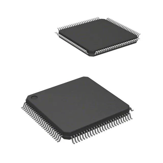
Core architecture and memory map
The LM3S1D21-IQC80-A2: On-chip memory comprises 512 KB of Flash and 96 KB of SRAM — the Flash is sized for moderate application code plus a bootloader, while the SRAM supports a real-time OS heap and multiple DMA buffers without external memory.
The connectivity block includes I²C, SPI, SSI, UART/USART, IrDA, LINbus, Microwire, and an external bus interface (EBI/EMI) — the latter allows direct attachment of an external SRAM or NOR Flash without a glue-logic CPLD. On-chip peripherals include a brown-out detect, power-on reset, DMA controller, PWM outputs, and a watchdog timer. An 8-channel 12-bit ADC handles analog inputs from sensors or potentiometers without an external converter.
Texas Instruments has marked the LM3S1D21-IQC80-A2 as obsolete. New designs should migrate to a current-generation Cortex-M3 or M4 part with similar peripheral mapping.