Core and memory configuration
The LM3S1B21-IQC80-C5: Built around the ARM Cortex-M3 core, this 32-bit single-core MCU runs at 80 MHz. The 80 MHz clock rate sets the instruction throughput ceiling for control loops and protocol processing — the Cortex-M3 pipeline executes most instructions in a single cycle, so the effective MIPS rate is close to the clock speed for register-based operations. On-chip memory comprises 256 KB of Flash (256K x 8) for program storage and 96 KB of SRAM (96K x 8) for data. The 256 KB Flash is sufficient for a moderate application stack including a real-time OS, communication stacks, and application code; the 96 KB SRAM provides headroom for data buffers and stack space without external memory.
Package, temperature, and supply voltage
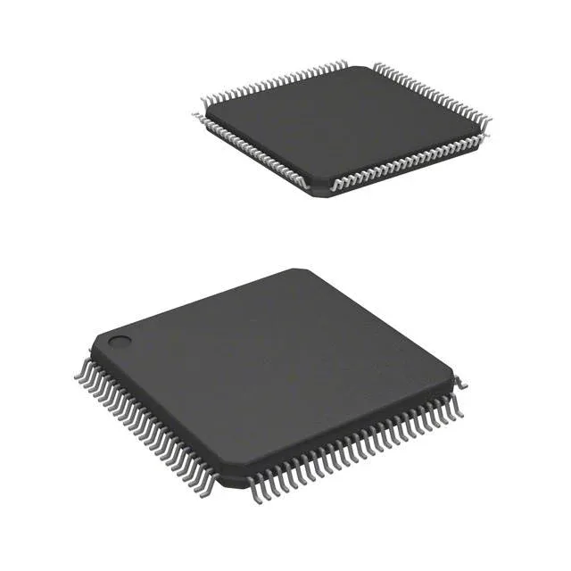
Housed in a 100-pin LQFP package (100-LQFP) with a 14x14 mm body.
Peripherals and connectivity
The device integrates a rich set of serial interfaces: I²C, SPI, SSI, UART/USART, IrDA, LINbus, and Microwire. The EBI/EMI interface allows connection to external memory or parallel peripherals, expanding the system beyond the on-chip resources. An 8-channel, 10-bit ADC handles analog sensor inputs. On-chip peripherals include brown-out detect/reset, DMA, POR, PWM, and a watchdog timer. The DMA controller offloads the CPU for data transfers between peripherals and memory, improving throughput in data-intensive applications like motor control or communication gateways.