Cortex-M3 at 80 MHz with 256 KB flash — what the memory map means for firmware
The LM3S1B21-IBZ80-C3: The 96 KB RAM is split across the core memory map — roughly 64 KB is available for code execution and data, with the remainder reserved for the Ethernet controller and USB FIFOs if those peripherals are active. For a firmware engineer, the 256 KB flash is enough for a full RTOS (FreeRTOS or TI-RTOS) plus a TCP/IP stack and application logic, but the 96 KB RAM is the tighter budget: a large frame buffer or a deep packet queue will eat into it fast. The part carries 67 general-purpose I/O pins, an internal oscillator, and a full set of brown-out detect, POR, DMA, PWM, and watchdog timers. The 8-channel 10-bit ADC is multiplexed onto the GPIO pads — you lose one analog input per channel used, but the mux is flexible enough to read eight single-ended signals without an external mux.
108-ball BGA — board-level layout considerations
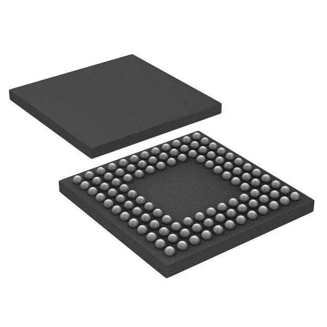
Housed in a 108-ball LFBGA with a 10x10 mm body and 0.80 mm ball pitch, this package routes out on two signal layers if the design stays within the inner ball field. The 0.80 mm pitch is forgiving enough for a standard 4-layer PCB with 0.2 mm trace/space — no microvias or HDI required. The supplier device package is 108-BGA (10x10), and the mounting is surface-mount only.
Texas Instruments lists the LM3S1B21-IBZ80-C3 as obsolete. For a design that already ships with this MCU, the 80 MHz Cortex-M3 core, the 256 KB flash footprint, and the 108-BGA package are the three parameters that define the board fit. Any pin-compatible replacement would need to match the ball map and the supply voltage range — without an official TI cross-reference, the safest path is to source the original part number through the surplus channel.